- 您现在的位置:买卖IC网 > PDF目录11732 > ORSO42G5-1BMN484I (Lattice Semiconductor Corporation)IC TRANCEIVERS FPSC 680FPGAM PDF资料下载
参数资料
| 型号: | ORSO42G5-1BMN484I |
| 厂商: | Lattice Semiconductor Corporation |
| 文件页数: | 106/153页 |
| 文件大小: | 0K |
| 描述: | IC TRANCEIVERS FPSC 680FPGAM |
| 产品变化通告: | Product Discontinuation 01/Aug/2011 |
| 标准包装: | 60 |
| 系列: | * |
第1页第2页第3页第4页第5页第6页第7页第8页第9页第10页第11页第12页第13页第14页第15页第16页第17页第18页第19页第20页第21页第22页第23页第24页第25页第26页第27页第28页第29页第30页第31页第32页第33页第34页第35页第36页第37页第38页第39页第40页第41页第42页第43页第44页第45页第46页第47页第48页第49页第50页第51页第52页第53页第54页第55页第56页第57页第58页第59页第60页第61页第62页第63页第64页第65页第66页第67页第68页第69页第70页第71页第72页第73页第74页第75页第76页第77页第78页第79页第80页第81页第82页第83页第84页第85页第86页第87页第88页第89页第90页第91页第92页第93页第94页第95页第96页第97页第98页第99页第100页第101页第102页第103页第104页第105页当前第106页第107页第108页第109页第110页第111页第112页第113页第114页第115页第116页第117页第118页第119页第120页第121页第122页第123页第124页第125页第126页第127页第128页第129页第130页第131页第132页第133页第134页第135页第136页第137页第138页第139页第140页第141页第142页第143页第144页第145页第146页第147页第148页第149页第150页第151页第152页第153页
Lattice Semiconductor
ORCA ORSO42G5 and ORSO82G5 Data Sheet
56
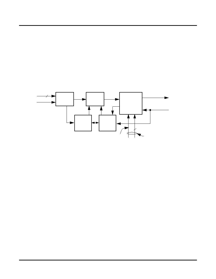
Cell Mode Receive Path
The receive logic blocks unique to the cell mode are shown in Figure 43 and are described in the next sections.
Prior to reaching this logic the received data has been demultiplexed, frame aligned and descrambled by the SER-
DES and SONET logic and is formatted on a per channel basis as 32-bit words with an accompanying clock. The
clock is a 77.76 MHz clock provided by the DEMUX block performing a divide-by-4 operation on RWCKxx.
The Data Extractor and receive FIFO (RXFIFO) process the data on a per channel basis. The receive FIFO also
performs a clock domain transfer to the 156 MHz domain of the Input Port Controller (IPC2/8) blocks. The IPC2/8
blocks perform the two-link or eight-link (ORSO82G5 only) alignment functions. In two-link alignment mode, the
received data are passed to the FPGA logic as 40-bit words at the 156 MHz rate. In eight-link alignment mode, the
received data are passed to the FPGA logic as a single 160-bit word, again at the 156 MHz rate. Additional mode-
dependent status information is also provided across the Core/FPGA interface.
Figure 43. Receive Path Logic Unique to Cell Mode
Cell Extractor
This block is used only in cell mode and does the following:
Extracts User cells from the SPE
Performs BIP calculation/checks to verify cell integrity
Link Header Sequence Interrogation
Processing options include:
Cell handling for invalid sequence (drop or pass to FPGA)
S/W congurable ‘link removal’ due to excessive sequence errors
Data from the cell extractor block(s) is sent to the receive FIFO which aligns the data to the system clock domain
and provides for deskew between the links.
Cell Extraction and BIP Calculation/Checking
The data from the descrambler are passed into the data extractor which strips the cell data from the payload of a
SONET frame. The block extracts the BIP value from the data stream and also perform an internal cell BIP calcula-
tion. If the BIP value is not correct, an error ag bit will set in the status registers. The block also determines when
the next Link Header is coming in the frame and what the cell sequence number contained within it should be. If the
value of the cell sequence counter is not equal to the expected value, an error ag bit will set in the status registers
and an error signal will be sent across the core/FPGA interface.
RX FIFO Data from Other Channel
Cell
Extractor
RX
FIFO
Write
IPC2
Control
FIFO
Read
Control
or
IPC8
Block
in Two-Link Alignment Group
RX FIFO Data from Other
Channels in Eight-Link
Alignment Group
IPC2_[A:B][1:2]
or IPC8
SYSCLK156[A:B][1:2]
or SYSCLK156 8
6
32
77.76 MHz
相关PDF资料 |
PDF描述 |
|---|---|
| V300A36E500BG2 | CONVERTER MOD DC/DC 36V 500W |
| VE-B00-IX-F1 | CONVERTER MOD DC/DC 5V 75W |
| ORSO42G5-2BMN484I | IC TRANCEIVERS FPSC 680FPGAM |
| ORSO42G5-1BMN484C | IC TRANCEIVERS FPSC 680FPGAM |
| VE-B03-IX-F1 | CONVERTER MOD DC/DC 24V 75W |
相关代理商/技术参数 |
参数描述 |
|---|---|
| ORSO42G5-2BM484C | 功能描述:FPGA - 现场可编程门阵列 10368 LUT 204 I/O RoHS:否 制造商:Altera Corporation 系列:Cyclone V E 栅极数量: 逻辑块数量:943 内嵌式块RAM - EBR:1956 kbit 输入/输出端数量:128 最大工作频率:800 MHz 工作电源电压:1.1 V 最大工作温度:+ 70 C 安装风格:SMD/SMT 封装 / 箱体:FBGA-256 |
| ORSO42G5-2BM484I | 功能描述:FPGA - 现场可编程门阵列 10368 LUT 204 I/O RoHS:否 制造商:Altera Corporation 系列:Cyclone V E 栅极数量: 逻辑块数量:943 内嵌式块RAM - EBR:1956 kbit 输入/输出端数量:128 最大工作频率:800 MHz 工作电源电压:1.1 V 最大工作温度:+ 70 C 安装风格:SMD/SMT 封装 / 箱体:FBGA-256 |
| ORSO42G5-2BMN484C | 功能描述:FPGA - 现场可编程门阵列 10368 LUT 204 I/O RoHS:否 制造商:Altera Corporation 系列:Cyclone V E 栅极数量: 逻辑块数量:943 内嵌式块RAM - EBR:1956 kbit 输入/输出端数量:128 最大工作频率:800 MHz 工作电源电压:1.1 V 最大工作温度:+ 70 C 安装风格:SMD/SMT 封装 / 箱体:FBGA-256 |
| ORSO42G5-2BMN484I | 功能描述:FPGA - 现场可编程门阵列 10368 LUT 204 I/O RoHS:否 制造商:Altera Corporation 系列:Cyclone V E 栅极数量: 逻辑块数量:943 内嵌式块RAM - EBR:1956 kbit 输入/输出端数量:128 最大工作频率:800 MHz 工作电源电压:1.1 V 最大工作温度:+ 70 C 安装风格:SMD/SMT 封装 / 箱体:FBGA-256 |
| ORSO42G5-3BM484C | 功能描述:FPGA - 现场可编程门阵列 10368 LUT 204 I/O RoHS:否 制造商:Altera Corporation 系列:Cyclone V E 栅极数量: 逻辑块数量:943 内嵌式块RAM - EBR:1956 kbit 输入/输出端数量:128 最大工作频率:800 MHz 工作电源电压:1.1 V 最大工作温度:+ 70 C 安装风格:SMD/SMT 封装 / 箱体:FBGA-256 |
发布紧急采购,3分钟左右您将得到回复。