- 您现在的位置:买卖IC网 > PDF目录11732 > ORSO42G5-1BMN484I (Lattice Semiconductor Corporation)IC TRANCEIVERS FPSC 680FPGAM PDF资料下载
参数资料
| 型号: | ORSO42G5-1BMN484I |
| 厂商: | Lattice Semiconductor Corporation |
| 文件页数: | 65/153页 |
| 文件大小: | 0K |
| 描述: | IC TRANCEIVERS FPSC 680FPGAM |
| 产品变化通告: | Product Discontinuation 01/Aug/2011 |
| 标准包装: | 60 |
| 系列: | * |
第1页第2页第3页第4页第5页第6页第7页第8页第9页第10页第11页第12页第13页第14页第15页第16页第17页第18页第19页第20页第21页第22页第23页第24页第25页第26页第27页第28页第29页第30页第31页第32页第33页第34页第35页第36页第37页第38页第39页第40页第41页第42页第43页第44页第45页第46页第47页第48页第49页第50页第51页第52页第53页第54页第55页第56页第57页第58页第59页第60页第61页第62页第63页第64页当前第65页第66页第67页第68页第69页第70页第71页第72页第73页第74页第75页第76页第77页第78页第79页第80页第81页第82页第83页第84页第85页第86页第87页第88页第89页第90页第91页第92页第93页第94页第95页第96页第97页第98页第99页第100页第101页第102页第103页第104页第105页第106页第107页第108页第109页第110页第111页第112页第113页第114页第115页第116页第117页第118页第119页第120页第121页第122页第123页第124页第125页第126页第127页第128页第129页第130页第131页第132页第133页第134页第135页第136页第137页第138页第139页第140页第141页第142页第143页第144页第145页第146页第147页第148页第149页第150页第151页第152页第153页
Lattice Semiconductor
ORCA ORSO42G5 and ORSO82G5 Data Sheet
19
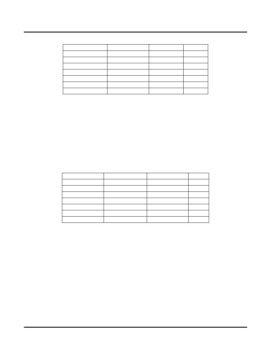
Table 2. Transmit PLL Clock and Data Rates
The receiver section receives high-speed serial data at its differential CML input port. These data are fed to the
clock recovery section which generates a recovered clock and retimes the data. This means that the receive clocks
are asynchronous between channels. The retimed data are deserialized and presented as a 8-bit parallel data on
the output port. RWCKx receive byte clocks are divide-by-4 clocks of the RBC (recovered byte clock) clock pro-
vided by the SERDES. This is the clock used in the internal receive functions of the embedded core.
The reference clock is also used by the receive PLL for operation when the input data are not toggling appropri-
ately. Table 3 shows the relationship between the data rates, the reference clock, and the RWCKx clocks.
Table 3. Receive PLL Clock and Data Rates
The differential reference clock is distributed to all channels in a SERDES block. Each channel has a differential
buffer to isolate the clock from the other channels. The input clock is preferably a differential signal; however, the
device can operate with a single-ended input. The input reference clock directly impacts the transmit data eye, so
the clock should have low jitter. In particular, jitter components in the DC-5 MHz range should be minimized.
Detailed Description - SERDES Only Mode
The SERDES only (or bypass) mode is the simplest of the three operating modes for the ORSO42G5 and
ORSO82G5. In this mode, all of the SONET and cell logic block functions are bypassed and data are transferred
directly between the MUX and DEMUX blocks to and from the FPGA interface. This mode is utilized when the user
wants to perform all data processing and uses only the SERDES portion of the Embedded Core. For example, this
mode could be utilized to replace an existing design using stand-alone SERDES and FPGAs.
The basic data paths in the transmit and receive directions are shown in Figure 5. In general, the descriptions in
this section are written to describe the SERDES only mode, although the “SERDES blocks” are also used in
SONET and cell mode operation. At the backplane interface, data are transmitted and received serially over pairs
Data Rate
Reference Clock
TCK78x
Rate
0.6 Gbps
75.00 MHz
18.75 MHz
Half
1.0 Gbps
125.00 MHz
31.25 MHz
Half
1.244 Gbps
155.52 MHz
38.88 MHz
Half
1.35 Gbps
168.75 MHz
42.19 MHz
Half
2.0 Gbps
125.00 MHz
61.50 MHz
Full
2.488 Gbps
155.52 MHz
77.76 MHz
Full
2.7 Gbps
168.75 MHz
84.38 MHz
Full
Notes:
1. The selection of full-rate or half-rate for a given reference clock speed is set by the TXHR
bit in the transmit control register and can be set per channel. (For cell mode all channels
of a group must have the same TXHR selection.)
Data Rate
Reference Clock
RWCKx Clocks
Rate
0.6 Gbps
75.00 MHz
18.75 MHz
Half
1.0 Gbps
125.00 MHz
31.25 MHz
Half
1.244 Gbps
155.52 MHz
38.88 MHz
Half
1.35 Gbps
168.75 MHz
42.19 MHz
Half
2.0 Gbps
125.00 MHz
61.50 MHz
Full
2.488 Gbps
155.52 MHz
77.76 MHz
Full
2.7 Gbps
168.75 MHz
84.38 MHz
Full
Note: The selection of full-rate or half-rate for a given reference clock speed is set by the
RXHR bit in the receive control register and can be set per channel. (For cell mode all chan-
nels of a group must have the same RXHR selection).
相关PDF资料 |
PDF描述 |
|---|---|
| V300A36E500BG2 | CONVERTER MOD DC/DC 36V 500W |
| VE-B00-IX-F1 | CONVERTER MOD DC/DC 5V 75W |
| ORSO42G5-2BMN484I | IC TRANCEIVERS FPSC 680FPGAM |
| ORSO42G5-1BMN484C | IC TRANCEIVERS FPSC 680FPGAM |
| VE-B03-IX-F1 | CONVERTER MOD DC/DC 24V 75W |
相关代理商/技术参数 |
参数描述 |
|---|---|
| ORSO42G5-2BM484C | 功能描述:FPGA - 现场可编程门阵列 10368 LUT 204 I/O RoHS:否 制造商:Altera Corporation 系列:Cyclone V E 栅极数量: 逻辑块数量:943 内嵌式块RAM - EBR:1956 kbit 输入/输出端数量:128 最大工作频率:800 MHz 工作电源电压:1.1 V 最大工作温度:+ 70 C 安装风格:SMD/SMT 封装 / 箱体:FBGA-256 |
| ORSO42G5-2BM484I | 功能描述:FPGA - 现场可编程门阵列 10368 LUT 204 I/O RoHS:否 制造商:Altera Corporation 系列:Cyclone V E 栅极数量: 逻辑块数量:943 内嵌式块RAM - EBR:1956 kbit 输入/输出端数量:128 最大工作频率:800 MHz 工作电源电压:1.1 V 最大工作温度:+ 70 C 安装风格:SMD/SMT 封装 / 箱体:FBGA-256 |
| ORSO42G5-2BMN484C | 功能描述:FPGA - 现场可编程门阵列 10368 LUT 204 I/O RoHS:否 制造商:Altera Corporation 系列:Cyclone V E 栅极数量: 逻辑块数量:943 内嵌式块RAM - EBR:1956 kbit 输入/输出端数量:128 最大工作频率:800 MHz 工作电源电压:1.1 V 最大工作温度:+ 70 C 安装风格:SMD/SMT 封装 / 箱体:FBGA-256 |
| ORSO42G5-2BMN484I | 功能描述:FPGA - 现场可编程门阵列 10368 LUT 204 I/O RoHS:否 制造商:Altera Corporation 系列:Cyclone V E 栅极数量: 逻辑块数量:943 内嵌式块RAM - EBR:1956 kbit 输入/输出端数量:128 最大工作频率:800 MHz 工作电源电压:1.1 V 最大工作温度:+ 70 C 安装风格:SMD/SMT 封装 / 箱体:FBGA-256 |
| ORSO42G5-3BM484C | 功能描述:FPGA - 现场可编程门阵列 10368 LUT 204 I/O RoHS:否 制造商:Altera Corporation 系列:Cyclone V E 栅极数量: 逻辑块数量:943 内嵌式块RAM - EBR:1956 kbit 输入/输出端数量:128 最大工作频率:800 MHz 工作电源电压:1.1 V 最大工作温度:+ 70 C 安装风格:SMD/SMT 封装 / 箱体:FBGA-256 |
发布紧急采购,3分钟左右您将得到回复。