- 您现在的位置:买卖IC网 > PDF目录367933 > PH28F256L18B85 (INTEL CORP) StrataFlash Wireless Memory PDF资料下载
参数资料
| 型号: | PH28F256L18B85 |
| 厂商: | INTEL CORP |
| 元件分类: | PROM |
| 英文描述: | StrataFlash Wireless Memory |
| 中文描述: | 16M X 16 FLASH 1.8V PROM, 85 ns, PBGA79 |
| 封装: | 0.75 MM PITCH, LEAD FREE, VFBGA-79 |
| 文件页数: | 21/106页 |
| 文件大小: | 1272K |
| 代理商: | PH28F256L18B85 |
第1页第2页第3页第4页第5页第6页第7页第8页第9页第10页第11页第12页第13页第14页第15页第16页第17页第18页第19页第20页当前第21页第22页第23页第24页第25页第26页第27页第28页第29页第30页第31页第32页第33页第34页第35页第36页第37页第38页第39页第40页第41页第42页第43页第44页第45页第46页第47页第48页第49页第50页第51页第52页第53页第54页第55页第56页第57页第58页第59页第60页第61页第62页第63页第64页第65页第66页第67页第68页第69页第70页第71页第72页第73页第74页第75页第76页第77页第78页第79页第80页第81页第82页第83页第84页第85页第86页第87页第88页第89页第90页第91页第92页第93页第94页第95页第96页第97页第98页第99页第100页第101页第102页第103页第104页第105页第106页
Intel StrataFlash Wireless Memory (L18)
Datasheet
Intel StrataFlash Wireless Memory (L18)
Order Number: 251902, Revision: 009
April 2005
21
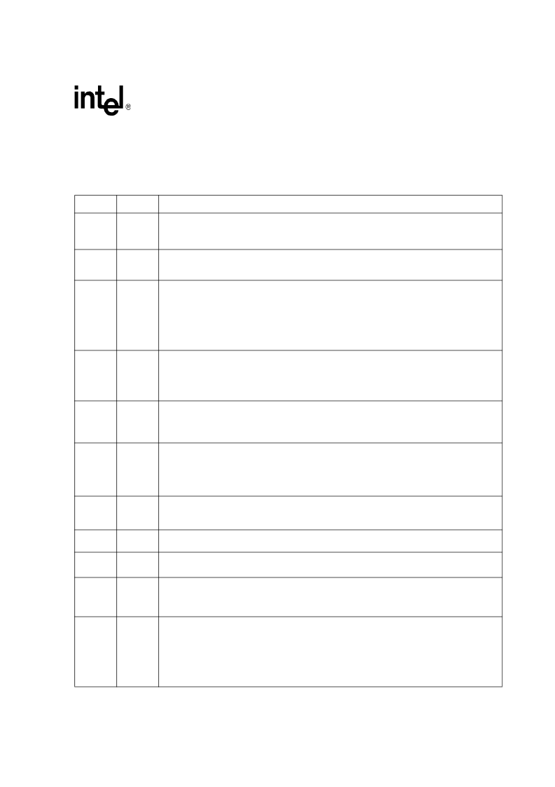
4.2.2
128/0 and 256/0 SCSP Package Signal Descriptions
Table 2
describes the active signals used on the 128/0 and 256/0 SCSP.
Table 2.
Device Signal Descriptions for SCSP (Sheet 1 of 2)
Symbol
Type
Description
A[Max:0]
Input
ADDRESS INPUTS:
Inputs for all die addresses during read and write operations.
128-Mbit Die: A[Max] = A22
256-Mbit Die: A[Max] = A23
DQ[15:0]
Input/
Output
DATA INPUTS/OUTPUTS:
Inputs data and commands during write cycles, outputs data during read
cycles. Data signals float when the device or its outputs are deselected. Data is internally latched
during writes.
F1-CE#
F2-CE#
F3-CE#
Input
FLASH CHIP ENABLE:
Low-true: selects the associated flash memory die. When asserted, flash
internal control logic, input buffers, decoders, and sense amplifiers are active. When deasserted, the
associated flash die is deselected, power is reduced to standby levels, data and WAIT outputs are
placed in high-Z state.
F1-CE# selects the flash die.
F2-CE# and F3-CE# are available on stacked combinations with two or three flash dies else they are
RFU. They each can be tied high to VCCQ through a 10K-ohm resistor for future design flexibility.
S-CS1#
S-CS2
Input
SRAM CHIP SELECTS:
When both SRAM chip selects are asserted, SRAM internal control logic,
input buffers, decoders, and sense amplifiers are active. When either/both SRAM chip selects are
deasserted (S-CS1# = V
IH
or S-CS2 = V
IL
), the SRAM is deselected and its power is reduced to
standby levels.
Treat this signal as NC (No Connect) for this device.
P-CS#
Input
PSRAM CHIP SELECT:
Low-true; when asserted, PSRAM internal control logic, input buffers,
decoders, and sense amplifiers are active. When deasserted, the PSRAM is deselected and its power
is reduced to standby levels.
Treat this signal as NC (No Connect) for this device.
F1-OE#
F2-OE#
Input
FLASH OUTPUT ENABLE:
Low-true; enables the flash output buffers. OE#-high disables the flash
output buffers, and places the flash outputs in High-Z.
F1-OE# controls the outputs of the flash die.
F2-OE# is available on stacked combinations with two or three flash dies else it is RFU. It can be
pulled high to VCCQ through a 10K-ohm resistor for future design flexibility.
R-OE#
Input
RAM OUTPUT ENABLE:
Low-true; R-OE#-low enables the selected RAM output buffers. R-OE#-high
disables the RAM output buffers, and places the selected RAM outputs in High-Z.
Treat this signal as NC (No Connect) for this device.
WE#
Input
FLASH WRITE ENABLE:
Low-true; WE# controls writes to the selected flash die. Address and data
are latched on the rising edge of WE#.
R-WE#
Input
RAM WRITE ENABLE:
Low-true; R-WE# controls writes to the selected RAM die.
Treat this signal as NC (No Connect) for this device.
CLK
Input
FLASH CLOCK:
Synchronizes the device with the system’s bus frequency in synchronous-read mode
and increments the internal address generator. During synchronous read operations, addresses are
latched on the rising edge of ADV#, or on the next valid CLK edge with ADV# low, whichever occurs
first.
WAIT
Output
FLASH WAIT:
Indicates data valid in synchronous array or non-array burst reads. Configuration
Register bit 10 (RCR[10], WT) determines its polarity when asserted. With CE# and OE# at V
,
WAIT’s active output is V
OL
or V
OH
when CE# and OE# are asserted. WAIT is high-Z if CE# or OE# is
V
IH
.
In synchronous array or non-array read modes, WAIT indicates invalid data when asserted and
valid data when deasserted.
In asynchronous page mode, and all write modes, WAIT is deasserted.
相关PDF资料 |
PDF描述 |
|---|---|
| PH28F256L18T85 | StrataFlash Wireless Memory |
| PH28F640L18B85 | StrataFlash Wireless Memory |
| PH28F640L18T85 | StrataFlash Wireless Memory |
| PH2907A | PNP switching transistor |
| PH2907 | PNP switching transistor |
相关代理商/技术参数 |
参数描述 |
|---|---|
| PH28F256L18B85A | 制造商:Micron Technology Inc 功能描述:MM#875138FLASH 28F256L18B 85 VF-PBGA79 S |
| PH28F256L18T85 | 制造商:INTEL 制造商全称:Intel Corporation 功能描述:StrataFlash Wireless Memory |
| PH28F320C3TD70A | 制造商:Micron Technology Inc 功能描述:Flash Mem Parallel 3V/3.3V 32M-Bit 2M x 16 70ns 48-Pin VFBGA Tray 制造商:Micron Technology Inc 功能描述:MM#869664FLASH 28F320C3TD 70 VF-PBGA47 E |
| PH28F320W18BE60A | 制造商:Micron Technology Inc 功能描述:IC FLASH 32MBIT 60NS VFBGA |
| PH28F320W18BE60B | 制造商:Micron Technology Inc 功能描述:32MB, CRYSTAL .75 VFBGA 1.8 LF - Tape and Reel |
发布紧急采购,3分钟左右您将得到回复。