- 您现在的位置:买卖IC网 > PDF目录10873 > PIC16C72-04E/SP (Microchip Technology)IC MCU OTP 2KX14 A/D PWM 28DIP PDF资料下载
参数资料
| 型号: | PIC16C72-04E/SP |
| 厂商: | Microchip Technology |
| 文件页数: | 100/114页 |
| 文件大小: | 0K |
| 描述: | IC MCU OTP 2KX14 A/D PWM 28DIP |
| 标准包装: | 15 |
| 系列: | PIC® 16C |
| 核心处理器: | PIC |
| 芯体尺寸: | 8-位 |
| 速度: | 4MHz |
| 连通性: | I²C,SPI |
| 外围设备: | 欠压检测/复位,POR,PWM,WDT |
| 输入/输出数: | 22 |
| 程序存储器容量: | 3.5KB(2K x 14) |
| 程序存储器类型: | OTP |
| RAM 容量: | 128 x 8 |
| 电压 - 电源 (Vcc/Vdd): | 4 V ~ 6 V |
| 数据转换器: | A/D 5x8b |
| 振荡器型: | 外部 |
| 工作温度: | -40°C ~ 125°C |
| 封装/外壳: | 28-DIP(0.300",7.62mm) |
| 包装: | 管件 |
第1页第2页第3页第4页第5页第6页第7页第8页第9页第10页第11页第12页第13页第14页第15页第16页第17页第18页第19页第20页第21页第22页第23页第24页第25页第26页第27页第28页第29页第30页第31页第32页第33页第34页第35页第36页第37页第38页第39页第40页第41页第42页第43页第44页第45页第46页第47页第48页第49页第50页第51页第52页第53页第54页第55页第56页第57页第58页第59页第60页第61页第62页第63页第64页第65页第66页第67页第68页第69页第70页第71页第72页第73页第74页第75页第76页第77页第78页第79页第80页第81页第82页第83页第84页第85页第86页第87页第88页第89页第90页第91页第92页第93页第94页第95页第96页第97页第98页第99页当前第100页第101页第102页第103页第104页第105页第106页第107页第108页第109页第110页第111页第112页第113页第114页
PIC16C7X
DS30390E-page 86
1997 Microchip Technology Inc.
To enable the serial port, SSP Enable bit, SSPEN
(SSPCON<5>) must be set. To reset or recongure SPI
mode, clear bit SSPEN, re-initialize the SSPCON reg-
ister, and then set bit SSPEN. This congures the SDI,
SDO, SCK, and SS pins as serial port pins. For the pins
to behave as the serial port function, they must have
their data direction bits (in the TRISC register) appro-
priately programmed. That is:
SDI must have TRISC<4> set
SDO must have TRISC<5> cleared
SCK (Master mode) must have TRISC<3>
cleared
SCK (Slave mode) must have TRISC<3> set
SS must have TRISA<5> set
Any serial port function that is not desired may be over-
ridden by programming the corresponding data direc-
tion (TRIS) register to the opposite value. An example
would be in master mode where you are only sending
data (to a display driver), then both SDI and SS could
be used as general purpose outputs by clearing their
corresponding TRIS register bits.
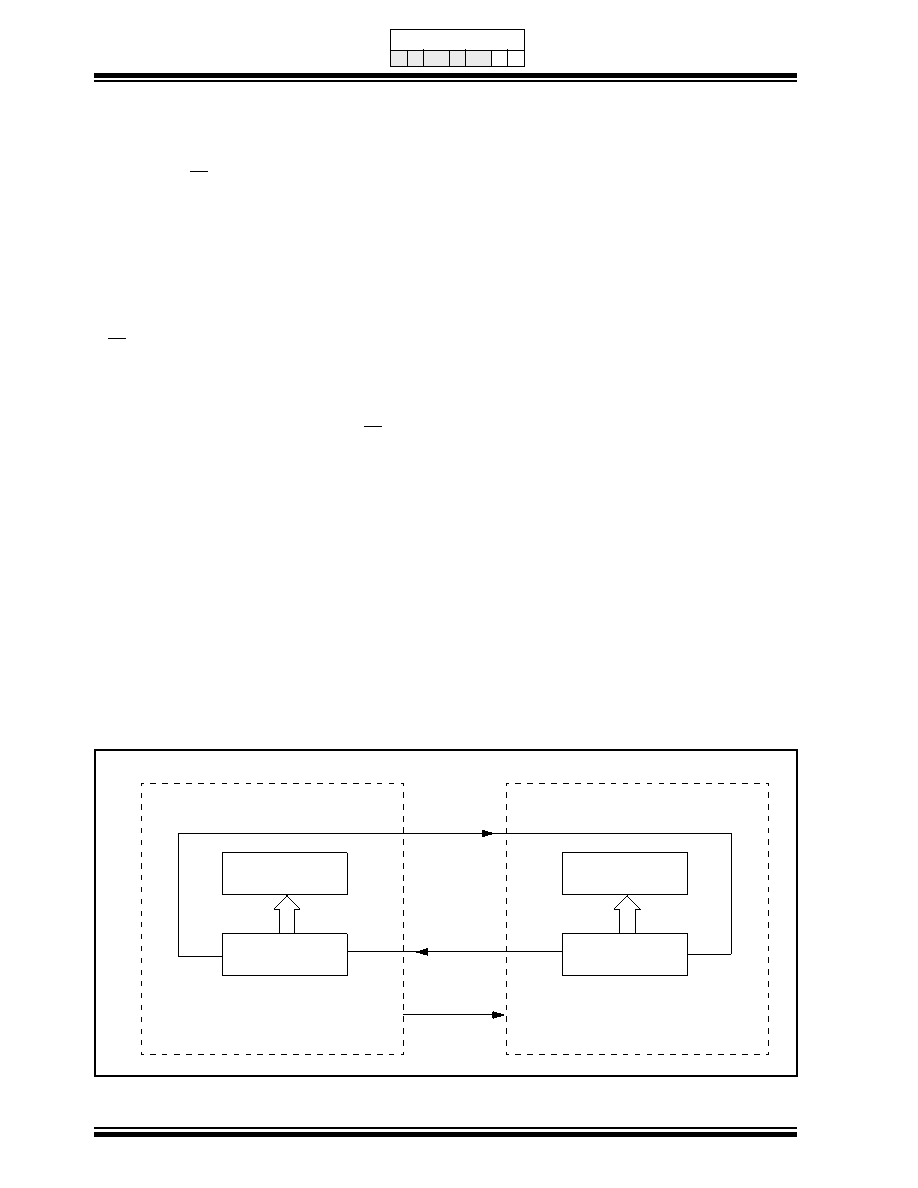
Figure 11-10 shows a typical connection between two
microcontrollers. The master controller (Processor 1)
initiates the data transfer by sending the SCK signal.
Data is shifted out of both shift registers on their pro-
grammed clock edge, and latched on the opposite edge
of the clock. Both processors should be programmed to
same Clock Polarity (CKP), then both controllers would
send and receive data at the same time. Whether the
data is meaningful (or dummy data) depends on the
application rmware. This leads to three scenarios for
data transmission:
Master sends data — Slave sends dummy data
Master sends data — Slave sends data
Master sends dummy data — Slave sends data
The master can initiate the data transfer at any time
because it controls the SCK. The master determines
when the slave (Processor 2) is to broadcast data by
the rmware protocol.
In master mode the data is transmitted/received as
soon as the SSPBUF register is written to. If the SPI is
only going to receive, the SCK output could be disabled
(programmed as an input). The SSPSR register will
continue to shift in the signal present on the SDI pin at
the programmed clock rate. As each byte is received, it
will be loaded into the SSPBUF register as if a normal
received byte (interrupts and status bits appropriately
set). This could be useful in receiver applications as a
“line activity monitor” mode.
In slave mode, the data is transmitted and received as
the external clock pulses appear on SCK. When the
last bit is latched the interrupt ag bit SSPIF (PIR1<3>)
is set.
The clock polarity is selected by appropriately program-
ming bit CKP (SSPCON<4>). This then would give
waveforms for SPI communication as shown in
Figure 11-11, Figure 11-12, and Figure 11-13 where
the MSB is transmitted rst. In master mode, the SPI
clock rate (bit rate) is user programmable to be one of
the following:
FOSC/4 (or TCY)
FOSC/16 (or 4 TCY)
FOSC/64 (or 16 TCY)
Timer2 output/2
This allows a maximum bit clock frequency (at 20 MHz)
of 5 MHz. When in slave mode the external clock must
meet the minimum high and low times.
In sleep mode, the slave can transmit and receive data
and wake the device from sleep.
FIGURE 11-10: SPI MASTER/SLAVE CONNECTION (PIC16C76/77)
Serial Input Buffer
(SSPBUF)
Shift Register
(SSPSR)
MSb
LSb
SDO
SDI
PROCESSOR 1
SCK
SPI Master SSPM3:SSPM0 = 00xxb
Serial Input Buffer
(SSPBUF)
Shift Register
(SSPSR)
LSb
MSb
SDI
SDO
PROCESSOR 2
SCK
SPI Slave SSPM3:SSPM0 = 010xb
Serial Clock
Applicable Devices
72 73 73A 74 74A 76 77
相关PDF资料 |
PDF描述 |
|---|---|
| PIC16C72-04E/SO | IC MCU OTP 2KX14 A/D PWM 28SOIC |
| PIC16C71T-20/SO | IC MCU OTP 1KX14 A/D 18SOIC |
| PIC16C71T-20I/SO | IC MCU OTP 1KX14 A/D 18SOIC |
| VE-B1D-IV-S | CONVERTER MOD DC/DC 85V 150W |
| VE-B1B-IV-S | CONVERTER MOD DC/DC 95V 150W |
相关代理商/技术参数 |
参数描述 |
|---|---|
| PIC16C72-04I/SO | 功能描述:8位微控制器 -MCU 3.5KB 128 RAM 22 I/O RoHS:否 制造商:Silicon Labs 核心:8051 处理器系列:C8051F39x 数据总线宽度:8 bit 最大时钟频率:50 MHz 程序存储器大小:16 KB 数据 RAM 大小:1 KB 片上 ADC:Yes 工作电源电压:1.8 V to 3.6 V 工作温度范围:- 40 C to + 105 C 封装 / 箱体:QFN-20 安装风格:SMD/SMT |
| PIC16C72-04I/SP | 功能描述:8位微控制器 -MCU 3.5KB 128 RAM 22 I/O RoHS:否 制造商:Silicon Labs 核心:8051 处理器系列:C8051F39x 数据总线宽度:8 bit 最大时钟频率:50 MHz 程序存储器大小:16 KB 数据 RAM 大小:1 KB 片上 ADC:Yes 工作电源电压:1.8 V to 3.6 V 工作温度范围:- 40 C to + 105 C 封装 / 箱体:QFN-20 安装风格:SMD/SMT |
| PIC16C72-04I/SS | 功能描述:8位微控制器 -MCU 3.5KB 128 RAM 22 I/O RoHS:否 制造商:Silicon Labs 核心:8051 处理器系列:C8051F39x 数据总线宽度:8 bit 最大时钟频率:50 MHz 程序存储器大小:16 KB 数据 RAM 大小:1 KB 片上 ADC:Yes 工作电源电压:1.8 V to 3.6 V 工作温度范围:- 40 C to + 105 C 封装 / 箱体:QFN-20 安装风格:SMD/SMT |
| PIC16C72-04SP | 制造商:Microchip Technology Inc 功能描述: |
| PIC16C72-10/SO | 功能描述:8位微控制器 -MCU 3.5KB 128 RAM 22 I/O RoHS:否 制造商:Silicon Labs 核心:8051 处理器系列:C8051F39x 数据总线宽度:8 bit 最大时钟频率:50 MHz 程序存储器大小:16 KB 数据 RAM 大小:1 KB 片上 ADC:Yes 工作电源电压:1.8 V to 3.6 V 工作温度范围:- 40 C to + 105 C 封装 / 箱体:QFN-20 安装风格:SMD/SMT |
发布紧急采购,3分钟左右您将得到回复。