- 您现在的位置:买卖IC网 > PDF目录10873 > PIC16C72-04E/SP (Microchip Technology)IC MCU OTP 2KX14 A/D PWM 28DIP PDF资料下载
参数资料
| 型号: | PIC16C72-04E/SP |
| 厂商: | Microchip Technology |
| 文件页数: | 94/114页 |
| 文件大小: | 0K |
| 描述: | IC MCU OTP 2KX14 A/D PWM 28DIP |
| 标准包装: | 15 |
| 系列: | PIC® 16C |
| 核心处理器: | PIC |
| 芯体尺寸: | 8-位 |
| 速度: | 4MHz |
| 连通性: | I²C,SPI |
| 外围设备: | 欠压检测/复位,POR,PWM,WDT |
| 输入/输出数: | 22 |
| 程序存储器容量: | 3.5KB(2K x 14) |
| 程序存储器类型: | OTP |
| RAM 容量: | 128 x 8 |
| 电压 - 电源 (Vcc/Vdd): | 4 V ~ 6 V |
| 数据转换器: | A/D 5x8b |
| 振荡器型: | 外部 |
| 工作温度: | -40°C ~ 125°C |
| 封装/外壳: | 28-DIP(0.300",7.62mm) |
| 包装: | 管件 |
第1页第2页第3页第4页第5页第6页第7页第8页第9页第10页第11页第12页第13页第14页第15页第16页第17页第18页第19页第20页第21页第22页第23页第24页第25页第26页第27页第28页第29页第30页第31页第32页第33页第34页第35页第36页第37页第38页第39页第40页第41页第42页第43页第44页第45页第46页第47页第48页第49页第50页第51页第52页第53页第54页第55页第56页第57页第58页第59页第60页第61页第62页第63页第64页第65页第66页第67页第68页第69页第70页第71页第72页第73页第74页第75页第76页第77页第78页第79页第80页第81页第82页第83页第84页第85页第86页第87页第88页第89页第90页第91页第92页第93页当前第94页第95页第96页第97页第98页第99页第100页第101页第102页第103页第104页第105页第106页第107页第108页第109页第110页第111页第112页第113页第114页
PIC16C7X
DS30390E-page 80
1997 Microchip Technology Inc.
11.2.1
OPERATION OF SSP MODULE IN SPI
MODE
The SPI mode allows 8-bits of data to be synchro-
nously transmitted and received simultaneously. To
accomplish communication, typically three pins are
used:
Serial Data Out (SDO)
Serial Data In (SDI)
Serial Clock (SCK)
Additionally a fourth pin may be used when in a slave
mode of operation:
Slave Select (SS)
When initializing the SPI, several options need to be
specied. This is done by programming the appropriate
control bits in the SSPCON register (SSPCON<5:0>).
These control bits allow the following to be specied:
Master Mode (SCK is the clock output)
Slave Mode (SCK is the clock input)
Clock Polarity (Output/Input data on the Rising/
Falling edge of SCK)
Clock Rate (Master mode only)
Slave Select Mode (Slave mode only)
The SSP consists of a transmit/receive Shift Register
(SSPSR) and a Buffer register (SSPBUF). The SSPSR
shifts the data in and out of the device, MSb rst. The
SSPBUF holds the data that was written to the SSPSR,
until the received data is ready. Once the 8-bits of data
have been received, that byte is moved to the SSPBUF
register. Then the Buffer Full bit, BF (SSPSTAT<0>)
and ag bit SSPIF are set. This double buffering of the
received data (SSPBUF) allows the next byte to start
reception before reading the data that was just
received. Any write to the SSPBUF register during
transmission/reception of data will be ignored, and the
write collision detect bit, WCOL (SSPCON<7>) will be
set. User software must clear bit WCOL so that it can
be determined if the following write(s) to the SSPBUF
completed successfully. When the application software
is expecting to receive valid data, the SSPBUF register
should be read before the next byte of data to transfer
is written to the SSPBUF register. The Buffer Full bit BF
(SSPSTAT<0>) indicates when the SSPBUF register
has been loaded with the received data (transmission
is complete). When the SSPBUF is read, bit BF is
cleared. This data may be irrelevant if the SPI is only a
transmitter. Generally the SSP Interrupt is used to
determine when the transmission/reception has com-
pleted. The SSPBUF register must be read and/or writ-
ten. If the interrupt method is not going to be used, then
software polling can be done to ensure that a write col-
lision does not occur. Example 11-1 shows the loading
of the SSPBUF (SSPSR) register for data transmission.
The shaded instruction is only required if the received
data is meaningful.
Applicable Devices
72 73 73A 74 74A 76 77
EXAMPLE 11-1: LOADING THE SSPBUF
(SSPSR) REGISTER
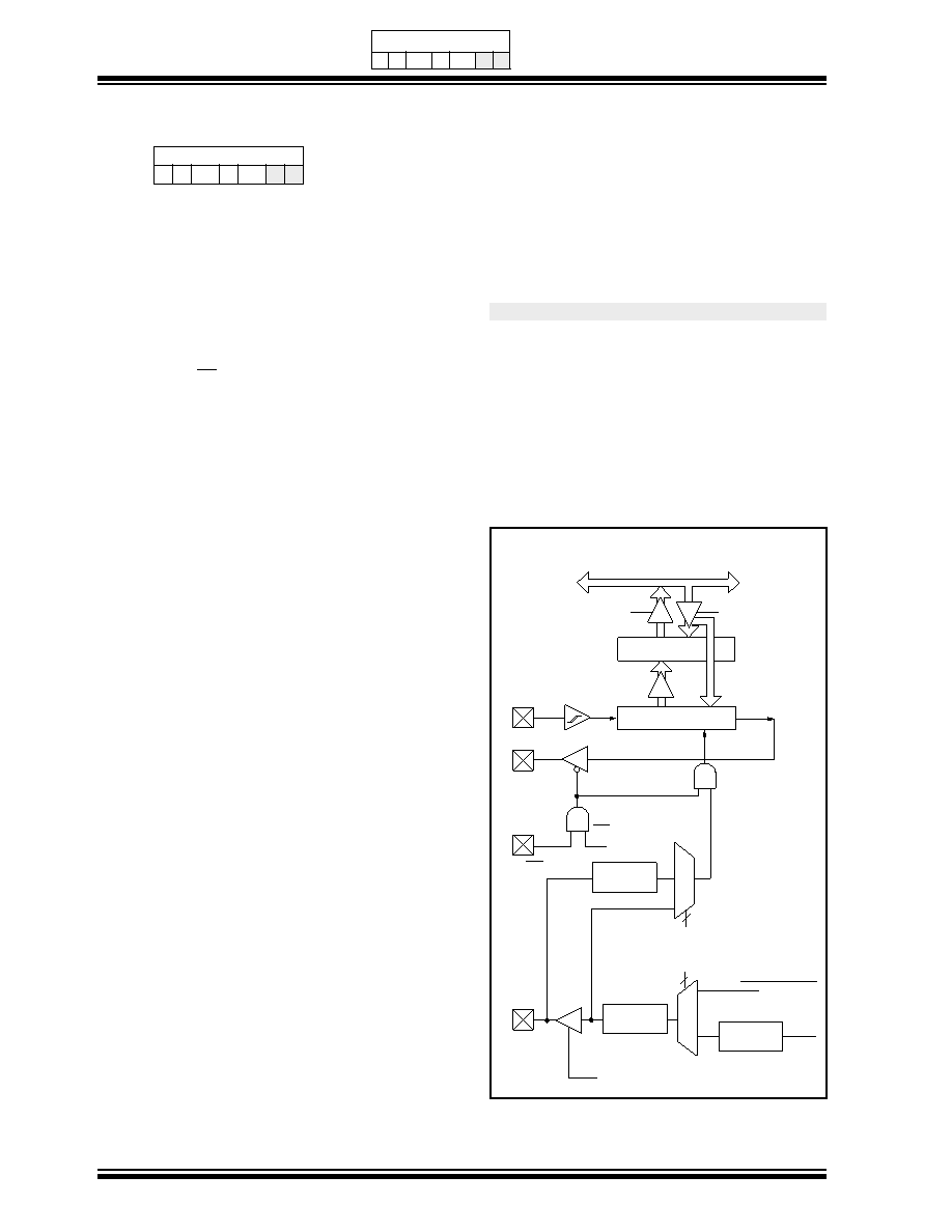
The block diagram of the SSP module, when in SPI
mode (Figure 11-3), shows that the SSPSR register is
not directly readable or writable, and can only be
accessed from addressing the SSPBUF register. Addi-
tionally, the SSP status register (SSPSTAT) indicates
the various status conditions.
FIGURE 11-3: SSP BLOCK DIAGRAM
(SPI MODE)
BSF
STATUS, RP0
;Specify Bank 1
LOOP BTFSS SSPSTAT, BF
;Has data been
;received
;(transmit
;complete)?
GOTO
LOOP
;No
BCF
STATUS, RP0
;Specify Bank 0
MOVF
SSPBUF, W
;W reg = contents
;of SSPBUF
MOVWF RXDATA
;Save in user RAM
MOVF
TXDATA, W
;W reg = contents
; of TXDATA
MOVWF SSPBUF
;New data to xmit
Read
Write
Internal
data bus
RC4/SDI/SDA
RC5/SDO
RA5/SS/AN4
RC3/SCK/
SSPSR reg
SSPBUF reg
SSPM3:SSPM0
bit0
shift
clock
SS Control
Enable
Edge
Select
Clock Select
TMR2 output
TCY
Prescaler
4, 16, 64
TRISC<3>
2
Edge
Select
2
4
SCL
Applicable Devices
72 73 73A 74 74A 76 77
相关PDF资料 |
PDF描述 |
|---|---|
| PIC16C72-04E/SO | IC MCU OTP 2KX14 A/D PWM 28SOIC |
| PIC16C71T-20/SO | IC MCU OTP 1KX14 A/D 18SOIC |
| PIC16C71T-20I/SO | IC MCU OTP 1KX14 A/D 18SOIC |
| VE-B1D-IV-S | CONVERTER MOD DC/DC 85V 150W |
| VE-B1B-IV-S | CONVERTER MOD DC/DC 95V 150W |
相关代理商/技术参数 |
参数描述 |
|---|---|
| PIC16C72-04I/SO | 功能描述:8位微控制器 -MCU 3.5KB 128 RAM 22 I/O RoHS:否 制造商:Silicon Labs 核心:8051 处理器系列:C8051F39x 数据总线宽度:8 bit 最大时钟频率:50 MHz 程序存储器大小:16 KB 数据 RAM 大小:1 KB 片上 ADC:Yes 工作电源电压:1.8 V to 3.6 V 工作温度范围:- 40 C to + 105 C 封装 / 箱体:QFN-20 安装风格:SMD/SMT |
| PIC16C72-04I/SP | 功能描述:8位微控制器 -MCU 3.5KB 128 RAM 22 I/O RoHS:否 制造商:Silicon Labs 核心:8051 处理器系列:C8051F39x 数据总线宽度:8 bit 最大时钟频率:50 MHz 程序存储器大小:16 KB 数据 RAM 大小:1 KB 片上 ADC:Yes 工作电源电压:1.8 V to 3.6 V 工作温度范围:- 40 C to + 105 C 封装 / 箱体:QFN-20 安装风格:SMD/SMT |
| PIC16C72-04I/SS | 功能描述:8位微控制器 -MCU 3.5KB 128 RAM 22 I/O RoHS:否 制造商:Silicon Labs 核心:8051 处理器系列:C8051F39x 数据总线宽度:8 bit 最大时钟频率:50 MHz 程序存储器大小:16 KB 数据 RAM 大小:1 KB 片上 ADC:Yes 工作电源电压:1.8 V to 3.6 V 工作温度范围:- 40 C to + 105 C 封装 / 箱体:QFN-20 安装风格:SMD/SMT |
| PIC16C72-04SP | 制造商:Microchip Technology Inc 功能描述: |
| PIC16C72-10/SO | 功能描述:8位微控制器 -MCU 3.5KB 128 RAM 22 I/O RoHS:否 制造商:Silicon Labs 核心:8051 处理器系列:C8051F39x 数据总线宽度:8 bit 最大时钟频率:50 MHz 程序存储器大小:16 KB 数据 RAM 大小:1 KB 片上 ADC:Yes 工作电源电压:1.8 V to 3.6 V 工作温度范围:- 40 C to + 105 C 封装 / 箱体:QFN-20 安装风格:SMD/SMT |
发布紧急采购,3分钟左右您将得到回复。