- 您现在的位置:买卖IC网 > PDF目录10873 > PIC16C72-04E/SP (Microchip Technology)IC MCU OTP 2KX14 A/D PWM 28DIP PDF资料下载
参数资料
| 型号: | PIC16C72-04E/SP |
| 厂商: | Microchip Technology |
| 文件页数: | 16/114页 |
| 文件大小: | 0K |
| 描述: | IC MCU OTP 2KX14 A/D PWM 28DIP |
| 标准包装: | 15 |
| 系列: | PIC® 16C |
| 核心处理器: | PIC |
| 芯体尺寸: | 8-位 |
| 速度: | 4MHz |
| 连通性: | I²C,SPI |
| 外围设备: | 欠压检测/复位,POR,PWM,WDT |
| 输入/输出数: | 22 |
| 程序存储器容量: | 3.5KB(2K x 14) |
| 程序存储器类型: | OTP |
| RAM 容量: | 128 x 8 |
| 电压 - 电源 (Vcc/Vdd): | 4 V ~ 6 V |
| 数据转换器: | A/D 5x8b |
| 振荡器型: | 外部 |
| 工作温度: | -40°C ~ 125°C |
| 封装/外壳: | 28-DIP(0.300",7.62mm) |
| 包装: | 管件 |
第1页第2页第3页第4页第5页第6页第7页第8页第9页第10页第11页第12页第13页第14页第15页当前第16页第17页第18页第19页第20页第21页第22页第23页第24页第25页第26页第27页第28页第29页第30页第31页第32页第33页第34页第35页第36页第37页第38页第39页第40页第41页第42页第43页第44页第45页第46页第47页第48页第49页第50页第51页第52页第53页第54页第55页第56页第57页第58页第59页第60页第61页第62页第63页第64页第65页第66页第67页第68页第69页第70页第71页第72页第73页第74页第75页第76页第77页第78页第79页第80页第81页第82页第83页第84页第85页第86页第87页第88页第89页第90页第91页第92页第93页第94页第95页第96页第97页第98页第99页第100页第101页第102页第103页第104页第105页第106页第107页第108页第109页第110页第111页第112页第113页第114页
PIC16C7X
DS30390E-page 112
1997 Microchip Technology Inc.
12.3.2
USART SYNCHRONOUS MASTER
RECEPTION
Once Synchronous mode is selected, reception is
enabled
by
setting
either
enable
bit
SREN
(RCSTA<5>) or enable bit CREN (RCSTA<4>). Data is
sampled on the RC7/RX/DT pin on the falling edge of
the clock. If enable bit SREN is set, then only a single
word is received. If enable bit CREN is set, the recep-
tion is continuous until CREN is cleared. If both bits are
set then CREN takes precedence. After clocking the
last bit, the received data in the Receive Shift Register
(RSR) is transferred to the RCREG register (if it is
empty). When the transfer is complete, interrupt ag bit
RCIF (PIR1<5>) is set. The actual interrupt can be
enabled/disabled by setting/clearing enable bit RCIE
(PIE1<5>). Flag bit RCIF is a read only bit which is
reset by the hardware. In this case it is reset when the
RCREG register has been read and is empty. The
RCREG is a double buffered register, i.e. it is a two
deep FIFO. It is possible for two bytes of data to be
received and transferred to the RCREG FIFO and a
third byte to begin shifting into the RSR register. On the
clocking of the last bit of the third byte, if the RCREG
register is still full then overrun error bit OERR
(RCSTA<1>) is set. The word in the RSR will be lost.
The RCREG register can be read twice to retrieve the
two bytes in the FIFO. Bit OERR has to be cleared in
software (by clearing bit CREN). If bit OERR is set,
transfers from the RSR to the RCREG are inhibited, so
it is essential to clear bit OERR if it is set. The 9th
receive bit is buffered the same way as the receive
data. Reading the RCREG register, will load bit RX9D
with a new value, therefore it is essential for the user to
read the RCSTA register before reading RCREG in
order not to lose the old RX9D information.
Steps to follow when setting up a Synchronous Master
Reception:
1.
Initialize the SPBRG register for the appropriate
baud rate. (Section 12.1)
2.
Enable the synchronous master serial port by
setting bits SYNC, SPEN, and CSRC.
3.
Ensure bits CREN and SREN are clear.
4.
If interrupts are desired, then set enable bit
RCIE.
5.
If 9-bit reception is desired, then set bit RX9.
6.
If a single reception is required, set bit SREN.
For continuous reception set bit CREN.
7.
Interrupt ag bit RCIF will be set when reception
is complete and an interrupt will be generated if
enable bit RCIE was set.
8.
Read the RCSTA register to get the ninth bit (if
enabled) and determine if any error occurred
during reception.
9.
Read the 8-bit received data by reading the
RCREG register.
10. If any error occurred, clear the error by clearing
bit CREN.
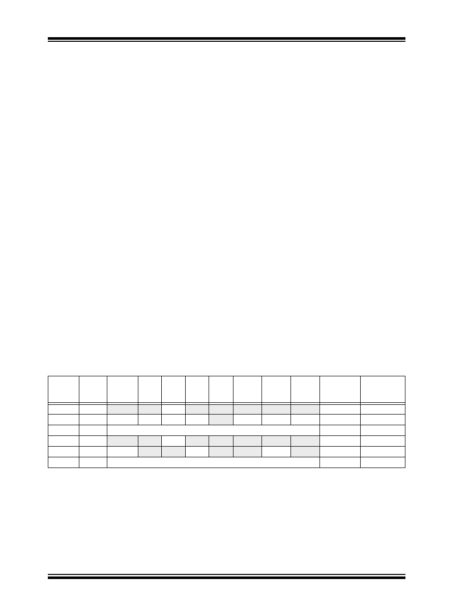
TABLE 12-9:
REGISTERS ASSOCIATED WITH SYNCHRONOUS MASTER RECEPTION
Address
Name
Bit 7
Bit 6
Bit 5
Bit 4
Bit 3
Bit 2
Bit 1
Bit 0
Value on:
POR,
BOR
Value on all
other Resets
0Ch
PIR1
PSPIF(1)
ADIF
RCIF
TXIF
SSPIF
CCP1IF
TMR2IF
TMR1IF
0000 0000
18h
RCSTA
SPEN
RX9
SREN
CREN
—
FERR
OERR
RX9D
0000 -00x
1Ah
RCREG
USART Receive Register
0000 0000
8Ch
PIE1
PSPIE(1)
ADIE
RCIE
TXIE
SSPIE
CCP1IE
TMR2IE
TMR1IE
0000 0000
98h
TXSTA
CSRC
TX9
TXEN
SYNC
—
BRGH
TRMT
TX9D
0000 -010
99h
SPBRG
Baud Rate Generator Register
0000 0000
Legend: x = unknown, - = unimplemented read as '0'. Shaded cells are not used for Synchronous Master Reception.
Note 1:
Bits PSPIE and PSPIF are reserved on the PIC16C73/73A/76, always maintain these bits clear.
相关PDF资料 |
PDF描述 |
|---|---|
| PIC16C72-04E/SO | IC MCU OTP 2KX14 A/D PWM 28SOIC |
| PIC16C71T-20/SO | IC MCU OTP 1KX14 A/D 18SOIC |
| PIC16C71T-20I/SO | IC MCU OTP 1KX14 A/D 18SOIC |
| VE-B1D-IV-S | CONVERTER MOD DC/DC 85V 150W |
| VE-B1B-IV-S | CONVERTER MOD DC/DC 95V 150W |
相关代理商/技术参数 |
参数描述 |
|---|---|
| PIC16C72-04I/SO | 功能描述:8位微控制器 -MCU 3.5KB 128 RAM 22 I/O RoHS:否 制造商:Silicon Labs 核心:8051 处理器系列:C8051F39x 数据总线宽度:8 bit 最大时钟频率:50 MHz 程序存储器大小:16 KB 数据 RAM 大小:1 KB 片上 ADC:Yes 工作电源电压:1.8 V to 3.6 V 工作温度范围:- 40 C to + 105 C 封装 / 箱体:QFN-20 安装风格:SMD/SMT |
| PIC16C72-04I/SP | 功能描述:8位微控制器 -MCU 3.5KB 128 RAM 22 I/O RoHS:否 制造商:Silicon Labs 核心:8051 处理器系列:C8051F39x 数据总线宽度:8 bit 最大时钟频率:50 MHz 程序存储器大小:16 KB 数据 RAM 大小:1 KB 片上 ADC:Yes 工作电源电压:1.8 V to 3.6 V 工作温度范围:- 40 C to + 105 C 封装 / 箱体:QFN-20 安装风格:SMD/SMT |
| PIC16C72-04I/SS | 功能描述:8位微控制器 -MCU 3.5KB 128 RAM 22 I/O RoHS:否 制造商:Silicon Labs 核心:8051 处理器系列:C8051F39x 数据总线宽度:8 bit 最大时钟频率:50 MHz 程序存储器大小:16 KB 数据 RAM 大小:1 KB 片上 ADC:Yes 工作电源电压:1.8 V to 3.6 V 工作温度范围:- 40 C to + 105 C 封装 / 箱体:QFN-20 安装风格:SMD/SMT |
| PIC16C72-04SP | 制造商:Microchip Technology Inc 功能描述: |
| PIC16C72-10/SO | 功能描述:8位微控制器 -MCU 3.5KB 128 RAM 22 I/O RoHS:否 制造商:Silicon Labs 核心:8051 处理器系列:C8051F39x 数据总线宽度:8 bit 最大时钟频率:50 MHz 程序存储器大小:16 KB 数据 RAM 大小:1 KB 片上 ADC:Yes 工作电源电压:1.8 V to 3.6 V 工作温度范围:- 40 C to + 105 C 封装 / 箱体:QFN-20 安装风格:SMD/SMT |
发布紧急采购,3分钟左右您将得到回复。