- 您现在的位置:买卖IC网 > PDF目录378056 > PM73487 (PMC-SIERRA INC) 622 Mbps ATM Traffic Management Device PDF资料下载
参数资料
| 型号: | PM73487 |
| 厂商: | PMC-SIERRA INC |
| 元件分类: | 数字传输电路 |
| 英文描述: | 622 Mbps ATM Traffic Management Device |
| 中文描述: | ATM/SONET/SDH SUPPORT CIRCUIT, PBGA503 |
| 封装: | EPBGA-503 |
| 文件页数: | 102/251页 |
| 文件大小: | 3126K |
| 代理商: | PM73487 |
第1页第2页第3页第4页第5页第6页第7页第8页第9页第10页第11页第12页第13页第14页第15页第16页第17页第18页第19页第20页第21页第22页第23页第24页第25页第26页第27页第28页第29页第30页第31页第32页第33页第34页第35页第36页第37页第38页第39页第40页第41页第42页第43页第44页第45页第46页第47页第48页第49页第50页第51页第52页第53页第54页第55页第56页第57页第58页第59页第60页第61页第62页第63页第64页第65页第66页第67页第68页第69页第70页第71页第72页第73页第74页第75页第76页第77页第78页第79页第80页第81页第82页第83页第84页第85页第86页第87页第88页第89页第90页第91页第92页第93页第94页第95页第96页第97页第98页第99页第100页第101页当前第102页第103页第104页第105页第106页第107页第108页第109页第110页第111页第112页第113页第114页第115页第116页第117页第118页第119页第120页第121页第122页第123页第124页第125页第126页第127页第128页第129页第130页第131页第132页第133页第134页第135页第136页第137页第138页第139页第140页第141页第142页第143页第144页第145页第146页第147页第148页第149页第150页第151页第152页第153页第154页第155页第156页第157页第158页第159页第160页第161页第162页第163页第164页第165页第166页第167页第168页第169页第170页第171页第172页第173页第174页第175页第176页第177页第178页第179页第180页第181页第182页第183页第184页第185页第186页第187页第188页第189页第190页第191页第192页第193页第194页第195页第196页第197页第198页第199页第200页第201页第202页第203页第204页第205页第206页第207页第208页第209页第210页第211页第212页第213页第214页第215页第216页第217页第218页第219页第220页第221页第222页第223页第224页第225页第226页第227页第228页第229页第230页第231页第232页第233页第234页第235页第236页第237页第238页第239页第240页第241页第242页第243页第244页第245页第246页第247页第248页第249页第250页第251页
PM73487 QRT
PMC-Sierra, Inc.
PMC-980618
Issue 3
622 Mbps ATMTraffic Management Device
Released
Datasheet
90
6.4
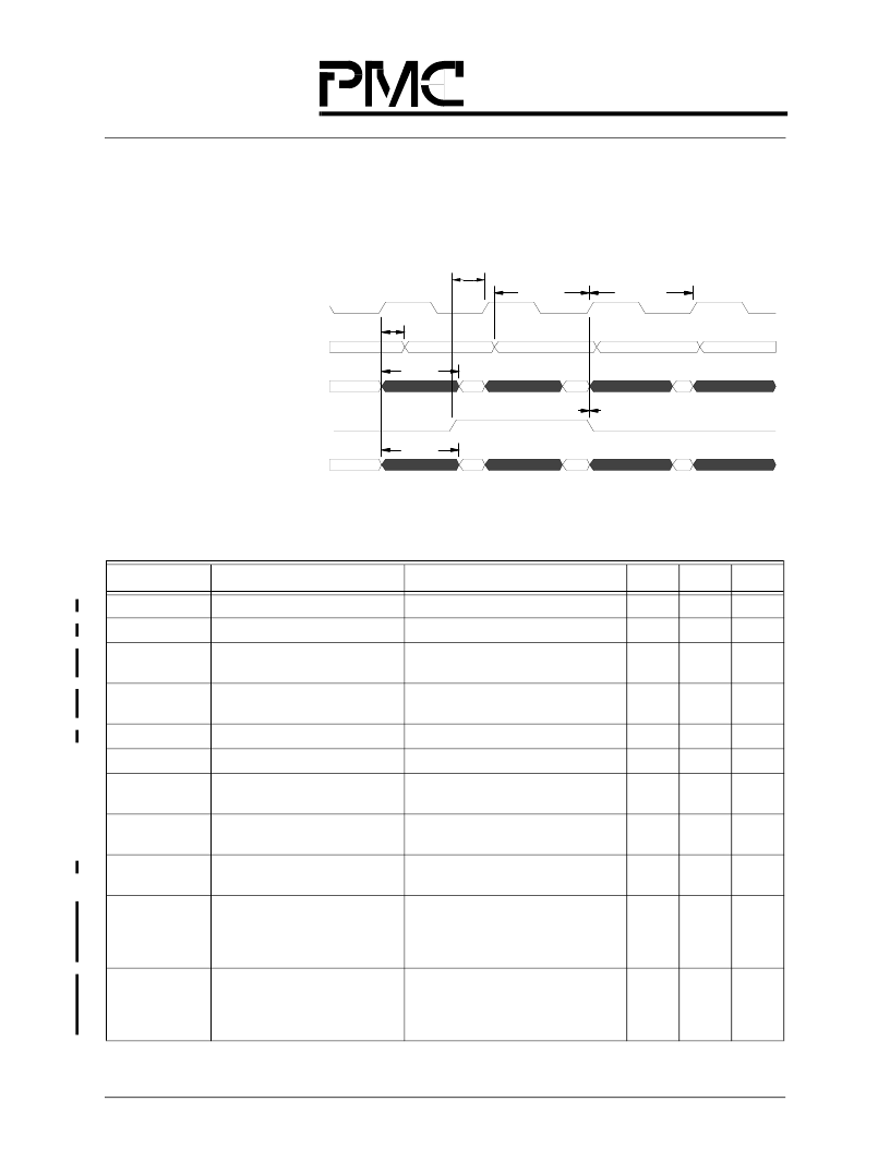
Output timing delays assume a capacitive loading of 30 pF on SE_D_OUT(3:0,3:0) and 48 pF on
SE_SOC_OUT. Figure 62 shows the bit-level timing for the QRT..
QRT-QSE Interface Timing
Figure 62. QRT Bit-Level Timing
Symbol
Parameter
Signals
Min
Max
Unit
Fseclk**
Frequency of SE_CLK
SE_CLK
65.4
68
MHz
clock duty cycle
SE_CLK
40
60
%
<10 KHz Jitter tolerance *
BP_ACK_IN(3:0), SE_SOC_IN(3:0)
2
clock
period
>10 KHz Jitter tolerance *
BP_ACK_IN(3:0), SE_SOC_IN(3:0)
0.35
clock
period
Tctsu
Control signal setup time
RX_CELL_START
1.5
ns
Tctho
Control signal hold time
RX_CELL_START
0
ns
Tsesu*
Setup time before SE_CLK
SE_D_IN(3:0,3:0), SE_SOC_IN(3:0),
BP_ACK_IN(3:0)
4.0
ns
Tseho*
Hold time after SE_CLK
SE_D_IN(3:0,3:0), SE_SOC_IN(3:0),
BP_ACK_IN(3:0)
1.5
ns
Tseq
Output delay from SE_CLK
SE_D_OUT(3:0,3:0),
BP_ACK_OUT(3:0), SE_SOC_OUT
2.9
10.0
ns
Output delay skew *
SE_D_OUT(0,3:0) and SE_SOC_OUT
SE_D_OUT(1,3:0) and SE_SOC_OUT
SE_D_OUT(2,3:0) and SE_SOC_OUT
SE_D_OUT(3,3:0) and SE_SOC_OUT
1.3
ns
Input delay skew *
SE_D_IN(0,3:0) and SE_SOC_IN(0)
SE_D_IN(1,3:0) and SE_SOC_IN(1)
SE_D_IN(2,3:0) and SE_SOC_IN(2)
SE_D_IN(3,3:0) and SE_SOC_IN(3)
3
ns
Tctsu
Tsesu
Fseclk
Tseho
Tseq
Tctho
Tseq
SE_CLK
SE_D_IN(3:0,3:0), BP_ACK_IN(3:0)
SE_D_OUT(3:0,3:0), BP_ACK_OUT(3:0)
RX_CELL_START
SE_SOC_OUT
相关PDF资料 |
PDF描述 |
|---|---|
| PM73488-PI | 5 Gbit/s ATM Switch Fabric Element |
| PM73488 | 5 Gbit/s ATM Switch Fabric Element |
| PM7349 | Ultraframer DS3/E3/DS2/E2/DS1/E1/DS0 |
| PM7350 | Dual Serial Link, PHY Multiplexer |
| PM7350-PI | DUAL SERIAL LINK PHY MULTIPLEXER |
相关代理商/技术参数 |
参数描述 |
|---|---|
| PM73487-PI | 制造商:PMC 制造商全称:PMC 功能描述:622 Mbps ATM Traffic Management Device |
| PM73488 | 制造商:PMC 制造商全称:PMC 功能描述:5 Gbit/s ATM Switch Fabric Element |
| PM73488PI | 制造商:未知厂家 制造商全称:未知厂家 功能描述:Telecommunication IC |
发布紧急采购,3分钟左右您将得到回复。