- 您现在的位置:买卖IC网 > PDF目录225140 > S29CL032J0JFAM020 (SPANSION LLC) 1M X 32 FLASH 3.3V PROM, 54 ns, PBGA80 PDF资料下载
参数资料
| 型号: | S29CL032J0JFAM020 |
| 厂商: | SPANSION LLC |
| 元件分类: | PROM |
| 英文描述: | 1M X 32 FLASH 3.3V PROM, 54 ns, PBGA80 |
| 封装: | 13 X 11 MM, 1 MM PITCH, FORTIFIED, BGA-80 |
| 文件页数: | 19/79页 |
| 文件大小: | 2994K |
| 代理商: | S29CL032J0JFAM020 |
第1页第2页第3页第4页第5页第6页第7页第8页第9页第10页第11页第12页第13页第14页第15页第16页第17页第18页当前第19页第20页第21页第22页第23页第24页第25页第26页第27页第28页第29页第30页第31页第32页第33页第34页第35页第36页第37页第38页第39页第40页第41页第42页第43页第44页第45页第46页第47页第48页第49页第50页第51页第52页第53页第54页第55页第56页第57页第58页第59页第60页第61页第62页第63页第64页第65页第66页第67页第68页第69页第70页第71页第72页第73页第74页第75页第76页第77页第78页第79页
26
S29CD-J & S29CL-J Flash Family
S29CD-J_CL-J_00_B3 March 30, 2009
Da ta
Sh e e t
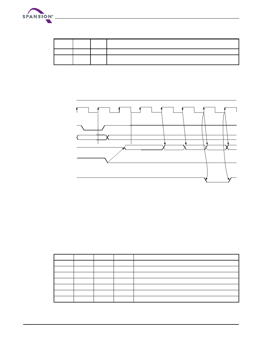
Figure 8.3 End of Burst Indicator (IND/WAIT#) Timing for Linear 4 Double Word Burst Operation
Note
Operation is shown for the 32-bit data bus. Figure shown with 3-CLK initial access delay configuration, linear address, 4-doubleword burst,
output on rising CLK edge, data hold for 1-CLK, IND/WAIT# asserted on the last transfer before wrap-around.
8.4.2
Initial Burst Access Delay
Initial Burst Access Delay is defined as the number of clock cycles that must elapse from the first valid clock
edge after ADV# assertion (or the rising edge of ADV#) until the first valid CLK edge when the data is valid.
Burst access is initiated and the address is latched on the first rising CLK edge when ADV# is active or upon
a rising ADV# edge, whichever comes first. The Initial Burst Access Delay is determined in the Configuration
Register (CR13-CR10). Refer to Table 8.5 for the initial access delay configurations under CR13-CR10. See
Figure 8.4 for the Initial Burst Delay Control timing diagram. Note that the Initial Access Delay for a burst
access has no effect on asynchronous read operations.
Table 8.3 Valid Configuration Register Bit Definition for IND/WAIT#
CR9
(DOC)
CR8
(WC)
CR6
(CC)
Definition
0
1
IND/WAIT# = VIL for 1-CLK cycle, Active on last transfer, Driven on rising CLK edge
01
1
IND/WAIT# = VIL for 1-CLK cycle, Active on second to last transfer, Driven on rising
CLK edge
CE#
CLK
ADV#
Addresses
OE#
Data
Address 1
Address 2
Invalid
D1
D2
D3
D0
Address 1 Latched
3 Clock Delay
IND/WAIT#
VIL
VIH
Table 8.4 Burst Initial Access Delay
CR13
CR12
CR11
CR10
Initial Burst Access (CLK cycles)
000
1
3
001
0
4
001
1
5
010
0
6
010
1
7
0
1
0
8
011
1
9
相关PDF资料 |
PDF描述 |
|---|---|
| S29CL032J0JFFM020 | 1M X 32 FLASH 3.3V PROM, 54 ns, PBGA80 |
| S29CL032J0RFAM012 | 1M X 32 FLASH 3.3V PROM, 48 ns, PBGA80 |
| S29GL032A10TAIR11 | Ceramic Chip Capacitors / High Voltage; Capacitance [nom]: 3.3pF; Working Voltage (Vdc)[max]: 500V; Capacitance Tolerance: +/-10%; Dielectric: Multilayer Ceramic; Temperature Coefficient: C0G (NP0); Lead Style: Surface Mount Chip; Lead Dimensions: 0805; Termination: Solder (SnPb) Plated Nickel Barrier; Body Dimensions: 0.079" x 0.049"; Container: Bulk; Features: High Voltage; Unmarked |
| S29GL032A10TAIR21 | 64 MEGABIT 32MEGABIT 3.0 BOLT ONLY PAGE MODE FLASH MEMORY |
| S29GL032A11BFIR31 | 64 MEGABIT 32MEGABIT 3.0 BOLT ONLY PAGE MODE FLASH MEMORY |
相关代理商/技术参数 |
参数描述 |
|---|---|
| S29CL032J0MFAI030 | 制造商:Spansion 功能描述:32MBIT FLASH - Trays |
| S29CL032J0PQFM010 | 制造商:Spansion 功能描述: 制造商:Spansion 功能描述:32MBIT FLASH - Tape and Reel |
| S29CL032J0RFAM010 | 制造商:Spansion 功能描述: |
| S29GL016A | 制造商:SPANSION 制造商全称:SPANSION 功能描述:64 Megabit, 32 Megabit, and 16 Megabit 3.0-Volt only Page Mode Flash Memory Featuring 200 nm MirrorBit Process Technology |
| S29GL016A100BAI010 | 制造商:SPANSION 制造商全称:SPANSION 功能描述:64 Megabit, 32 Megabit, and 16 Megabit 3.0-Volt only Page Mode Flash Memory Featuring 200 nm MirrorBit Process Technology |
发布紧急采购,3分钟左右您将得到回复。