- 您现在的位置:买卖IC网 > PDF目录225140 > S29CL032J0JFAM020 (SPANSION LLC) 1M X 32 FLASH 3.3V PROM, 54 ns, PBGA80 PDF资料下载
参数资料
| 型号: | S29CL032J0JFAM020 |
| 厂商: | SPANSION LLC |
| 元件分类: | PROM |
| 英文描述: | 1M X 32 FLASH 3.3V PROM, 54 ns, PBGA80 |
| 封装: | 13 X 11 MM, 1 MM PITCH, FORTIFIED, BGA-80 |
| 文件页数: | 71/79页 |
| 文件大小: | 2994K |
| 代理商: | S29CL032J0JFAM020 |
第1页第2页第3页第4页第5页第6页第7页第8页第9页第10页第11页第12页第13页第14页第15页第16页第17页第18页第19页第20页第21页第22页第23页第24页第25页第26页第27页第28页第29页第30页第31页第32页第33页第34页第35页第36页第37页第38页第39页第40页第41页第42页第43页第44页第45页第46页第47页第48页第49页第50页第51页第52页第53页第54页第55页第56页第57页第58页第59页第60页第61页第62页第63页第64页第65页第66页第67页第68页第69页第70页当前第71页第72页第73页第74页第75页第76页第77页第78页第79页
March 30, 2009 S29CD-J_CL-J_00_B3
S29CD-J & S29CL-J Flash Family
73
Data
She e t
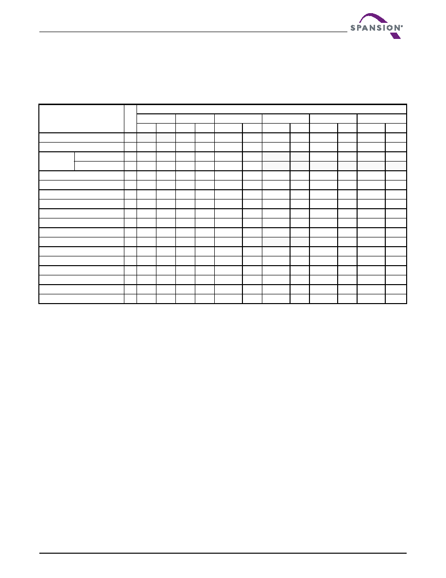
20. Appendix 2
20.1
Command Definitions
Legend
Notes
Table 20.1 Memory Array Command Definitions (x32 Mode)
Command (Notes)
Cy
c
le
s
Bus Cycles (Notes 1–4)
First
Second
Third
Fourth
Fifth
Sixth
Addr
Data
Addr
Data
Addr
Data
Addr
Data
Addr
Data
Addr
Data
Read (5)1
RA
RD
Reset (6)1
XXX
F0
Autoselect
(7)
Manufacturer ID
4
555
AA
2AA
55
555
90
BA+X00
01
Device ID (8)
6
555
AA
2AA
55
555
90
BA+X01
7E
BA+X0E
09
BA+X0F
00/01
Program
4
555
AA
2AA
55
555
A0
PA
PD
Chip Erase
6
555
AA
2AA
55
555
80
555
AA
2AA
55
555
10
Sector Erase
6
555
AA
2AA
55
555
80
555
AA
2AA
55
SA
30
Program/Erase Suspend (9)1
BA
B0
Program/Erase Resume (10)1
BA
30
55
98
Accelerated Program (13)
2
XX
A0
PA
PD
Configuration Register Verify (12)
3
555
AA
2AA
55
BA+555
C6
BA+XX
RD
Configuration Register Write (14)
4
555
AA
2AA
55
555
D0
XX
WD
Unlock Bypass Entry (15)
3
555
AA
2AA
55
555
20
Unlock Bypass Program (15)
2
XX
A0
PA
PD
Unlock Bypass Erase (15)
2
XX
80
XX
10
XX
98
Unlock Bypass Reset (15)
2
XX
90
XX
00
BA = Bank Address. The set of addresses that comprise a bank. The system may
write any address within a bank to identify that bank for a command.
PA = Program Address (Amax–A0). Addresses latch on the falling edge of the
WE# or CE# pulse, whichever happens later.
PD = Program Data (DQmax–DQ0) written to location PA. Data latches on the
rising edge of WE# or CE# pulse, whichever happens first.
RA = Read Address (Amax–A0).
RD = Read Data. Data DQmax–DQ0 at address location RA.
SA = Sector Address. The set of addresses that comprise a sector. The system
may write any address within a sector to identify that sector for a command.
WD = Write Data. See “Configuration Register” definition for specific write data.
Data latched on rising edge of WE#.
X = Don’t care
1. See Table 8.1 for description of bus operations.
2. All values are in hexadecimal.
3. Shaded cells in table denote read cycles. All other cycles are write
operations.
4. During unlock cycles, (lower address bits are 555 or 2AAh as shown in table)
address bits higher than A11 (except where BA is required) and data bits
higher than DQ7 are don’t cares.
5. No unlock or command cycles required when bank is reading array data.
6. The Reset command is required to return to the read mode (or to the erase-
suspend-read mode if previously in Erase Suspend) when a bank is in the
autoselect mode, or if DQ5 goes high (while the bank is providing status
information).
7. The fourth cycle of the autoselect command sequence is a read cycle. The
system must provide the bank address to obtain the manufacturer ID or
device ID information. See “Autoselect” for more information.
8. The device ID must be read across the fourth, fifth, and sixth cycles. 00h in
the sixth cycle indicates ordering option 00, 01h indicates ordering option 01.
9. The system may read and program in non-erasing sectors when in the
Program/Erase Suspend mode. The Program/Erase Suspend command is
valid only during a sector erase operation, and requires the bank address.
10. The Program/Erase Resume command is valid only during the Erase
Suspend mode, and requires the bank address.
11. Command is valid when device is ready to read array data.
12. Asynchronous read operations.
13. ACC must be at VID during the entire operation of this command.
14. Command is ignored during any Embedded Program, Embedded Erase, or
Suspend operation.
15. The Unlock Bypass Entry command is required prior to any Unlock Bypass
operation. The Unlock Bypass Reset command is required to return to the
read mode.
相关PDF资料 |
PDF描述 |
|---|---|
| S29CL032J0JFFM020 | 1M X 32 FLASH 3.3V PROM, 54 ns, PBGA80 |
| S29CL032J0RFAM012 | 1M X 32 FLASH 3.3V PROM, 48 ns, PBGA80 |
| S29GL032A10TAIR11 | Ceramic Chip Capacitors / High Voltage; Capacitance [nom]: 3.3pF; Working Voltage (Vdc)[max]: 500V; Capacitance Tolerance: +/-10%; Dielectric: Multilayer Ceramic; Temperature Coefficient: C0G (NP0); Lead Style: Surface Mount Chip; Lead Dimensions: 0805; Termination: Solder (SnPb) Plated Nickel Barrier; Body Dimensions: 0.079" x 0.049"; Container: Bulk; Features: High Voltage; Unmarked |
| S29GL032A10TAIR21 | 64 MEGABIT 32MEGABIT 3.0 BOLT ONLY PAGE MODE FLASH MEMORY |
| S29GL032A11BFIR31 | 64 MEGABIT 32MEGABIT 3.0 BOLT ONLY PAGE MODE FLASH MEMORY |
相关代理商/技术参数 |
参数描述 |
|---|---|
| S29CL032J0MFAI030 | 制造商:Spansion 功能描述:32MBIT FLASH - Trays |
| S29CL032J0PQFM010 | 制造商:Spansion 功能描述: 制造商:Spansion 功能描述:32MBIT FLASH - Tape and Reel |
| S29CL032J0RFAM010 | 制造商:Spansion 功能描述: |
| S29GL016A | 制造商:SPANSION 制造商全称:SPANSION 功能描述:64 Megabit, 32 Megabit, and 16 Megabit 3.0-Volt only Page Mode Flash Memory Featuring 200 nm MirrorBit Process Technology |
| S29GL016A100BAI010 | 制造商:SPANSION 制造商全称:SPANSION 功能描述:64 Megabit, 32 Megabit, and 16 Megabit 3.0-Volt only Page Mode Flash Memory Featuring 200 nm MirrorBit Process Technology |
发布紧急采购,3分钟左右您将得到回复。