- 您现在的位置:买卖IC网 > PDF目录85256 > SC103335VR400B (FREESCALE SEMICONDUCTOR INC) 32-BIT, 400 MHz, MICROPROCESSOR, PBGA272 PDF资料下载
参数资料
| 型号: | SC103335VR400B |
| 厂商: | FREESCALE SEMICONDUCTOR INC |
| 元件分类: | 微控制器/微处理器 |
| 英文描述: | 32-BIT, 400 MHz, MICROPROCESSOR, PBGA272 |
| 封装: | 27 X 27 MM, 1.27 MM PITCH, ROHS COMPLIANT, PLASTIC, BGA-272 |
| 文件页数: | 16/72页 |
| 文件大小: | 978K |
| 代理商: | SC103335VR400B |
第1页第2页第3页第4页第5页第6页第7页第8页第9页第10页第11页第12页第13页第14页第15页当前第16页第17页第18页第19页第20页第21页第22页第23页第24页第25页第26页第27页第28页第29页第30页第31页第32页第33页第34页第35页第36页第37页第38页第39页第40页第41页第42页第43页第44页第45页第46页第47页第48页第49页第50页第51页第52页第53页第54页第55页第56页第57页第58页第59页第60页第61页第62页第63页第64页第65页第66页第67页第68页第69页第70页第71页第72页
MPC5200B Data Sheet, Rev. 4
Freescale Semiconductor
23
2. Minimum times are measured at the package pin with the load circuit, and maximum times are measured with the load circuit
as shown in the PCI Local Bus Specification.
3. REQ# and GNT# are point-to-point signals and have different input setup times than do bused signals. GNT# and REQ# have
a setup of 5 ns at 66 MHz. All other signals are bused.
4. See the timing measurement conditions in the PCI Local Bus Specification.
For Measurement and Test Conditions, see the PCI Local Bus Specification.
1.3.8
Local Plus Bus
The Local Plus Bus is the external bus interface of the MPC5200B. A maximum of eight configurable chip selects (CS) are
provided. There are two main modes of operation: non-MUXed (Legacy and Burst) and MUXED. The reference clock is the
PCI CLK. The maximum bus frequency is 66 MHz.
Definition of Acronyms and Terms:
WS = Wait State
DC = Dead Cycle
LB = Long Burst
DS = Data Size in Bytes
tPCIck = PCI clock period
tIPBIck = IPBI clock period
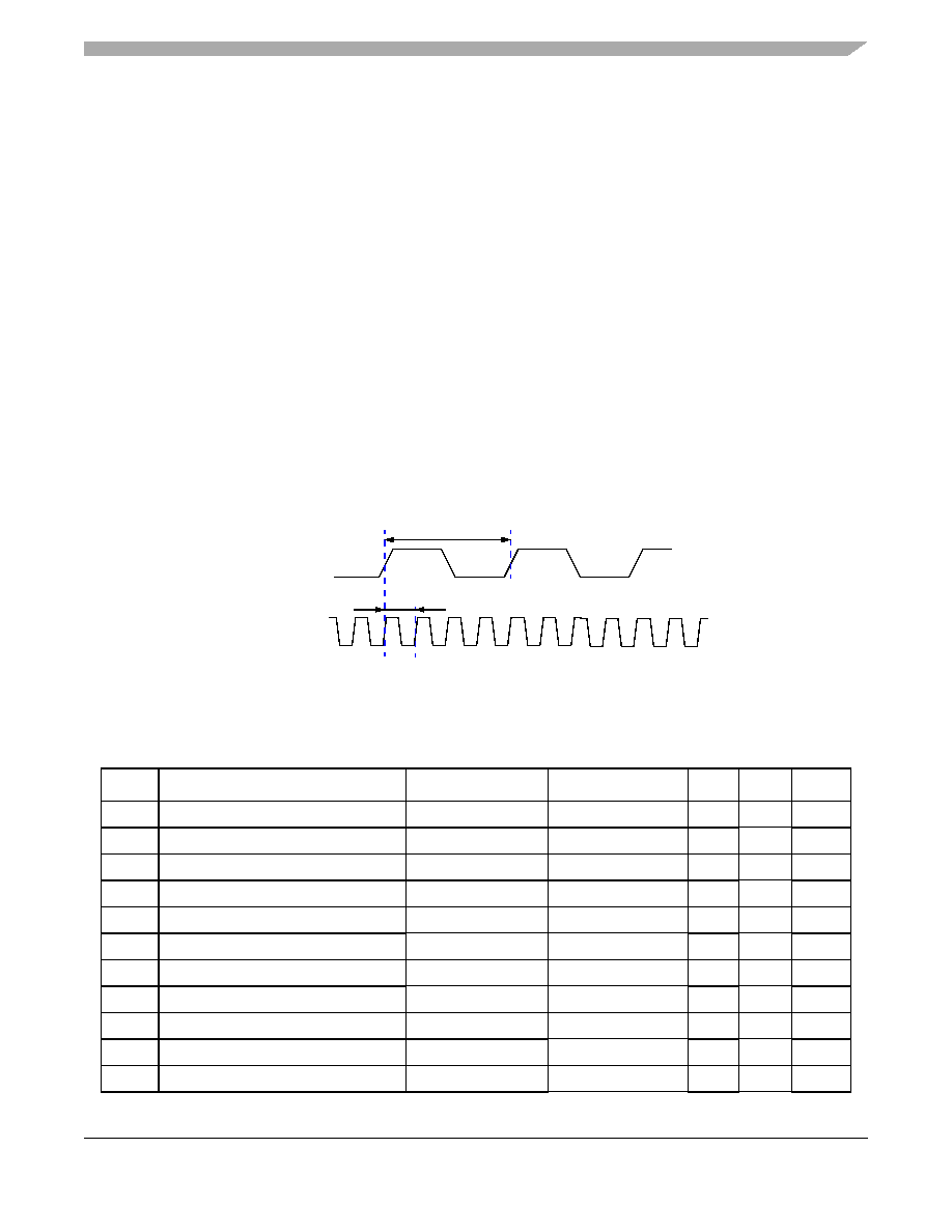
Figure 10. Timing Diagram—IPBI and PCI clock (example ratio: 4:1)
1.3.8.1
Non-MUXed Mode
Table 24. Non-MUXed Mode Timing
Sym
Description
Min
Max
Units
Notes
SpecID
tCSA
PCI CLK to CS assertion
4.6
10.6
ns
—A7.1
tCSN
PCI CLK to CS negation
2.9
7.0
ns
—A7.2
t1
CS pulse width
(2 + WS) × tPCIck
(2 +WS) ×tPCIck
ns
(1)
A7.3
t2
ADDR valid before CS assertion
tIPBIck
tPCIck
ns
—A7.4
t3
ADDR hold after CS negation
tIPBIck
—ns
(2)
A7.5
t4
OE assertion before CS assertion
—4.8
ns
—A7.6
t5
OE negation before CS negation
—2.7
ns
—A7.7
t6
RW valid before CS assertion
tPCIck
—ns
—A7.8
t7
RW hold after CS negation
tIPBIck
—ns
—A7.9
t8
DATA output valid before CS assertion
tIPBIck
—ns
—
A7.10
t9
DATA output hold after CS negation
tIPBIck
—ns
—
A7.11
PCI CLK
IPBI CLK
tIPBIck
tPCIck
相关PDF资料 |
PDF描述 |
|---|---|
| SAH-XC2265N-40F40L | 32-BIT, FLASH, 40 MHz, RISC MICROCONTROLLER, PQFP100 |
| SCN8032HCFA44 | 8-BIT, 7.5 MHz, MICROCONTROLLER, PQCC44 |
| S80C52UXXX-25 | 8-BIT, MROM, 25 MHz, MICROCONTROLLER, PQCC44 |
| S80C154U-S:D | 8-BIT, 20 MHz, MICROCONTROLLER, PQCC44 |
| S83C154UXXX-42:R | 8-BIT, MROM, 42 MHz, MICROCONTROLLER, PQCC44 |
相关代理商/技术参数 |
参数描述 |
|---|---|
| SC1034 | 制造商:未知厂家 制造商全称:未知厂家 功能描述:VOLTAGE REGULATOR |
| SC1036 | 制造商:National Semiconductor 功能描述:1036 |
| SC1037 | 制造商:未知厂家 制造商全称:未知厂家 功能描述:VOLTAGE REGULATOR |
| SC10371LB2 | 制造商:Motorola Inc 功能描述: |
| SC1-03770 | 制造商:Tamura Corporation of America 功能描述: |
发布紧急采购,3分钟左右您将得到回复。