- 您现在的位置:买卖IC网 > PDF目录85256 > SC103335VR400B (FREESCALE SEMICONDUCTOR INC) 32-BIT, 400 MHz, MICROPROCESSOR, PBGA272 PDF资料下载
参数资料
| 型号: | SC103335VR400B |
| 厂商: | FREESCALE SEMICONDUCTOR INC |
| 元件分类: | 微控制器/微处理器 |
| 英文描述: | 32-BIT, 400 MHz, MICROPROCESSOR, PBGA272 |
| 封装: | 27 X 27 MM, 1.27 MM PITCH, ROHS COMPLIANT, PLASTIC, BGA-272 |
| 文件页数: | 26/72页 |
| 文件大小: | 978K |
| 代理商: | SC103335VR400B |
第1页第2页第3页第4页第5页第6页第7页第8页第9页第10页第11页第12页第13页第14页第15页第16页第17页第18页第19页第20页第21页第22页第23页第24页第25页当前第26页第27页第28页第29页第30页第31页第32页第33页第34页第35页第36页第37页第38页第39页第40页第41页第42页第43页第44页第45页第46页第47页第48页第49页第50页第51页第52页第53页第54页第55页第56页第57页第58页第59页第60页第61页第62页第63页第64页第65页第66页第67页第68页第69页第70页第71页第72页
MPC5200B Data Sheet, Rev. 4
32
Freescale Semiconductor
NOTES:
1 tUI, tMLI, tLI indicate sender-to-recipient or recipient-to-sender interlocks. That is, one agent (sender or recipient) is waiting for
the other agent to respond with a signal before proceeding.
tUI is an unlimited interlock that has no maximum time value.
tMLI is a limited time-out that has a defined minimum.
tLI is a limited time-out that has a defined maximum.
2 All timing parameters are measured at the connector of the drive to which the parameter applies. For example, the sender shall
stop generating STROBE edges tRFS after negation of DMARDY. STROBE and DMARDY timing measurements are taken at
the connector of the sender. Even though the sender stops generating STROBE edges, the receiver may receive additional
STROBE edges due to propagation delays. All timing measurement switching points (low to high and high to low) are taken at
1.5 V.
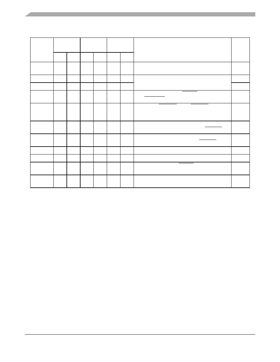
t AZ
—
10
—
10
—
10
Maximum time allowed for output drivers to release
from being asserted or negated
A8.36
tZAH
20
—
20
—
20
—
Minimum delay time required for output drivers to
assert or negate from released state
A8.37
t ZAD
0—0—0—
A8.38
t ENV
20
70
20
70
20
70
Envelope time—from DMACK to STOP and
HDMARDY during data out burst initiation.
A8.39
t SR
—
50
—
30
—
20
STROBE to DMARDY time, if DMARDY is negated
before this long after STROBE edge, the recipient
receives no more than one additional data word.
A8.40
t RFS
—
75
—
60
—
50
Ready-to-Final STROBE time—no STROBE edges
are sent this long after negation of DMARDY.
A8.41
t RP
160
—
125
—
100
—
Ready-to-Pause time—the time recipient waits to
initiate pause after negating DMARDY.
A8.42
t IORDYZ
—
20
—
20
—
20
Pull-up time before allowing IORDY to be released.
A8.43
t ZIORDY
0
—
0
—
0
—
Minimum time drive waits before driving IORDY
A8.44
t ACK
20
—
20
—
20
—
Setup and hold times for DMACK, before assertion or
negation.
A8.45
t SS
50
—
50
—
50
—
Time from STROBE edge to negation of DMARQ or
assertion of STOP, when sender terminates a burst.
A8.46
Table 29. Ultra DMA Timing Specification (continued)
Sym
MODE 0
(ns)
MODE 1
(ns)
MODE 2
(ns)
Comment
SpecID
Min
Max
Min
Max
Min
Max
相关PDF资料 |
PDF描述 |
|---|---|
| SAH-XC2265N-40F40L | 32-BIT, FLASH, 40 MHz, RISC MICROCONTROLLER, PQFP100 |
| SCN8032HCFA44 | 8-BIT, 7.5 MHz, MICROCONTROLLER, PQCC44 |
| S80C52UXXX-25 | 8-BIT, MROM, 25 MHz, MICROCONTROLLER, PQCC44 |
| S80C154U-S:D | 8-BIT, 20 MHz, MICROCONTROLLER, PQCC44 |
| S83C154UXXX-42:R | 8-BIT, MROM, 42 MHz, MICROCONTROLLER, PQCC44 |
相关代理商/技术参数 |
参数描述 |
|---|---|
| SC1034 | 制造商:未知厂家 制造商全称:未知厂家 功能描述:VOLTAGE REGULATOR |
| SC1036 | 制造商:National Semiconductor 功能描述:1036 |
| SC1037 | 制造商:未知厂家 制造商全称:未知厂家 功能描述:VOLTAGE REGULATOR |
| SC10371LB2 | 制造商:Motorola Inc 功能描述: |
| SC1-03770 | 制造商:Tamura Corporation of America 功能描述: |
发布紧急采购,3分钟左右您将得到回复。