- 您现在的位置:买卖IC网 > PDF目录98078 > SC1201UCL-266F (ADVANCED MICRO DEVICES INC) 32-BIT, 266 MHz, MICROPROCESSOR, PBGA432 PDF资料下载
参数资料
| 型号: | SC1201UCL-266F |
| 厂商: | ADVANCED MICRO DEVICES INC |
| 元件分类: | 微控制器/微处理器 |
| 英文描述: | 32-BIT, 266 MHz, MICROPROCESSOR, PBGA432 |
| 封装: | 40 X 40 MM, 1.72 MM HEIGHT, 1.27 MM PITCH, LEAD FREE, MO-151, EBGA-432 |
| 文件页数: | 84/465页 |
| 文件大小: | 4068K |
| 代理商: | SC1201UCL-266F |
第1页第2页第3页第4页第5页第6页第7页第8页第9页第10页第11页第12页第13页第14页第15页第16页第17页第18页第19页第20页第21页第22页第23页第24页第25页第26页第27页第28页第29页第30页第31页第32页第33页第34页第35页第36页第37页第38页第39页第40页第41页第42页第43页第44页第45页第46页第47页第48页第49页第50页第51页第52页第53页第54页第55页第56页第57页第58页第59页第60页第61页第62页第63页第64页第65页第66页第67页第68页第69页第70页第71页第72页第73页第74页第75页第76页第77页第78页第79页第80页第81页第82页第83页当前第84页第85页第86页第87页第88页第89页第90页第91页第92页第93页第94页第95页第96页第97页第98页第99页第100页第101页第102页第103页第104页第105页第106页第107页第108页第109页第110页第111页第112页第113页第114页第115页第116页第117页第118页第119页第120页第121页第122页第123页第124页第125页第126页第127页第128页第129页第130页第131页第132页第133页第134页第135页第136页第137页第138页第139页第140页第141页第142页第143页第144页第145页第146页第147页第148页第149页第150页第151页第152页第153页第154页第155页第156页第157页第158页第159页第160页第161页第162页第163页第164页第165页第166页第167页第168页第169页第170页第171页第172页第173页第174页第175页第176页第177页第178页第179页第180页第181页第182页第183页第184页第185页第186页第187页第188页第189页第190页第191页第192页第193页第194页第195页第196页第197页第198页第199页第200页第201页第202页第203页第204页第205页第206页第207页第208页第209页第210页第211页第212页第213页第214页第215页第216页第217页第218页第219页第220页第221页第222页第223页第224页第225页第226页第227页第228页第229页第230页第231页第232页第233页第234页第235页第236页第237页第238页第239页第240页第241页第242页第243页第244页第245页第246页第247页第248页第249页第250页第251页第252页第253页第254页第255页第256页第257页第258页第259页第260页第261页第262页第263页第264页第265页第266页第267页第268页第269页第270页第271页第272页第273页第274页第275页第276页第277页第278页第279页第280页第281页第282页第283页第284页第285页第286页第287页第288页第289页第290页第291页第292页第293页第294页第295页第296页第297页第298页第299页第300页第301页第302页第303页第304页第305页第306页第307页第308页第309页第310页第311页第312页第313页第314页第315页第316页第317页第318页第319页第320页第321页第322页第323页第324页第325页第326页第327页第328页第329页第330页第331页第332页第333页第334页第335页第336页第337页第338页第339页第340页第341页第342页第343页第344页第345页第346页第347页第348页第349页第350页第351页第352页第353页第354页第355页第356页第357页第358页第359页第360页第361页第362页第363页第364页第365页第366页第367页第368页第369页第370页第371页第372页第373页第374页第375页第376页第377页第378页第379页第380页第381页第382页第383页第384页第385页第386页第387页第388页第389页第390页第391页第392页第393页第394页第395页第396页第397页第398页第399页第400页第401页第402页第403页第404页第405页第406页第407页第408页第409页第410页第411页第412页第413页第414页第415页第416页第417页第418页第419页第420页第421页第422页第423页第424页第425页第426页第427页第428页第429页第430页第431页第432页第433页第434页第435页第436页第437页第438页第439页第440页第441页第442页第443页第444页第445页第446页第447页第448页第449页第450页第451页第452页第453页第454页第455页第456页第457页第458页第459页第460页第461页第462页第463页第464页第465页
174
AMD Geode SC1200/SC1201 Processor Data Book
Core Logic Module
Revision 7.1
DMA Addressing Capability
DMA transfers occur over the entire 32-bit address range of
the PCI bus. This is accomplished by using the DMA con-
troller’s 16-bit memory address registers in conjunction
with an 8-bit DMA Low Page register and an 8-bit DMA
High Page register. These registers, associated with each
channel, provide the 32-bit memory address capability. A
write to the Low Page register clears the High Page regis-
ter, for backward compatibility with the PC/AT standard.
The starting address for the DMA transfer must be pro-
grammed into the DMA controller registers and the chan-
nel’s respective Low and High Page registers prior to
beginning the DMA transfer.
DMA Page Registers and Extended Addressing
The DMA Page registers provide the upper address bits
during DMA cycles. DMA addresses do not increment or
decrement across page boundaries. Page boundaries for
the 8-bit channels (Channels 0 through 3) are every 64 KB
and page boundaries for the 16-bit channels (Channels 5,
6, and 7) are every 128 KB.
Before any DMA operations are performed, the Page regis-
ters must be written at the I/O Port addresses in the DMA
controller registers to select the correct page for each DMA
channel. The other address locations between 080h and
08Fh and 480h and 48Fh are not used by the DMA chan-
nels, but can be read or written by a PCI bus master. These
registers are reset to zero at POR. A write to the Low Page
register clears the High Page register, for backward com-
patibility with the PC/AT standard.
For most DMA transfers, the High Page register is set to
zeros and is driven onto PCI address bits AD[31:24] during
DMA cycles. This mode is backward compatible with the
PC/AT standard. For DMA extended transfers, the High
Page register is programmed and the values are driven
onto the PCI addresses AD[31:24] during DMA cycles to
allow access to the full 4 GB PCI address space.
DMA Address Generation
The DMA addresses are formed such that there is an
upper address, a middle address, and a lower address por-
tion.
The upper address portion, which selects a specific page,
is generated by the Page registers. The Page registers for
each channel must be set up by the system before a DMA
operation. The DMA Page register values are driven on
PCI address bits AD[31:16] for 8-bit channels and
AD[31:17] for 16-bit channels.
The middle address portion, which selects a block within
the page, is generated by the DMA controller at the begin-
ning of a DMA operation and any time the DMA address
increments or decrements through a block boundary. Block
sizes are 256 bytes for 8-bit channels (Channels 0 through
3) and 512 bytes for 16-bit channels (Channels 5, 6, and
7). The middle address bits are is driven on PCI address
bits AD[15:8] for 8-bit channels and AD[16:9] for 16-bit
channels.
The lower address portion is generated directly by the DMA
controller during DMA operations. The lower address bits
are output on PCI address bits AD[7:0] for 8-bit channels
and AD[8:1] for 16-bit channels.
BHE# is configured as an output during all DMA opera-
tions. It is driven as the inversion of AD0 during 8-bit DMA
cycles and forced low for all 16-bit DMA cycles.
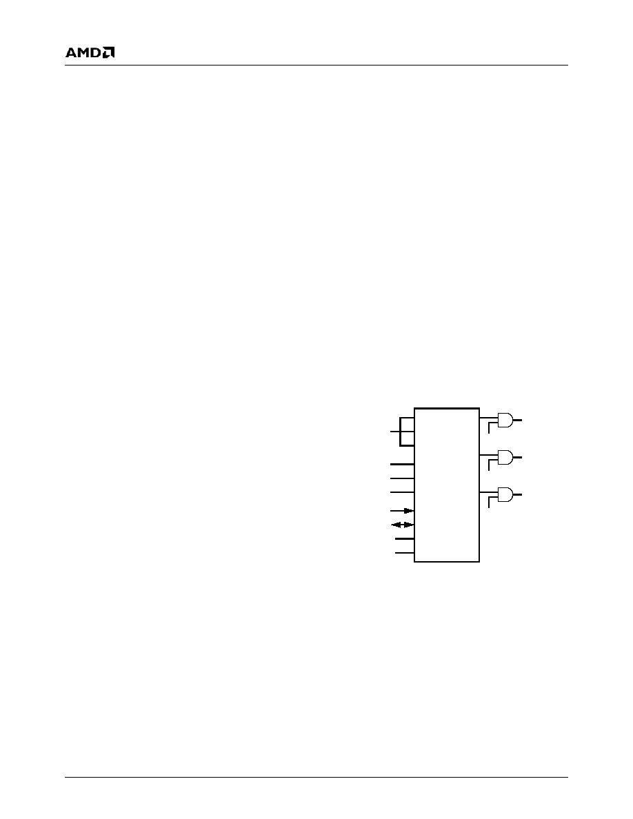
6.2.6.2
Programmable Interval Timer
The Core Logic module contains an 8254-equivalent Pro-
grammable Interval Timer (PIT) configured as shown in
Figure 6-7. The PIT has three timers/counters, each with
an input frequency of 1.19318 MHz (OSC divided by 12),
and individually programmable to different modes.
The gates of Counter 0 and 1 are usually enabled, how-
ever, they can be controlled via F0 Index 50h. The gate of
Counter 2 is connected to I/O Port 061h[0]. The output of
Counter 0 is connected internally to IRQ0. This timer is typ-
ically configured in Mode 3 (square wave output), and used
to generate IRQ0 at a periodic rate to be used as a system
timer function. The output of Counter 1 is connected to I/O
Port 061h[4]. The reset state of I/O Port 061h[4] is 0 and
every falling edge of Counter 1 output causes I/O Port
061h[4] to flip states. The output of Counter 2 is brought
out to the PC_BEEP output. This output is gated with I/O
Port 061h[1].
Figure 6-7. PIT Timer
PIT Shadow Register
The PIT registers are shadowed to allow for 0V Suspend to
save/restore the PIT state by reading the PIT’s counter and
write only registers. The read sequence for the shadow
register is listed in F0 Index BAh (see Table 6-29 on page
CLK0
CLK1
CLK2
GATE0
GATE1
GATE2
XD[7:0]
A[1:0]
IOW#
IOR#
I/O Port 061h[1]
I/O Port 061h[0]
IRQ0
I/O Port
PC_BEEP
1.19318 MHz
WR#
RD#
OUT0
OUT1
OUT2
F0 Index 50h[4]
F0 Index 50h[6]
F0 Index 50h[3]
F0 Index 50h[5]
061h[4]
相关PDF资料 |
PDF描述 |
|---|---|
| SC12484CV-80 | PALETTE-DAC DSPL CTLR, PQCC44 |
| SC11483CV-110 | PALETTE-DAC DSPL CTLR, PQCC44 |
| SC11483CV-80 | PALETTE-DAC DSPL CTLR, PQCC44 |
| SC12482CV-80 | PALETTE-DAC DSPL CTLR, PQCC44 |
| SC12483CV-66 | PALETTE-DAC DSPL CTLR, PQCC44 |
相关代理商/技术参数 |
参数描述 |
|---|---|
| SC1201UFH-266 | 制造商:Rochester Electronics LLC 功能描述:- Bulk 制造商:Advanced Micro Devices 功能描述: 制造商:AMD 功能描述: |
| SC1201UFH-266B | 制造商:Rochester Electronics LLC 功能描述:- Bulk |
| SC1201UFH-266F | 制造商:Rochester Electronics LLC 功能描述:- Bulk |
| SC1201UFH-266FR | 制造商:Rochester Electronics LLC 功能描述:- Bulk |
| SC1202 | 制造商:SEMTECH 制造商全称:Semtech Corporation 功能描述:600mA Low Dropout Positive Voltage Regulator |
发布紧急采购,3分钟左右您将得到回复。