参数资料
| 型号: | SC2544TSTRT |
| 厂商: | Semtech |
| 文件页数: | 13/22页 |
| 文件大小: | 0K |
| 描述: | IC REG CTRLR BUCK PWM VM 24TSSOP |
| 标准包装: | 1 |
| PWM 型: | 电压模式 |
| 输出数: | 2 |
| 频率 - 最大: | 300kHz |
| 占空比: | 90% |
| 电源电压: | 4.5 V ~ 28 V |
| 降压: | 是 |
| 升压: | 无 |
| 回扫: | 无 |
| 反相: | 无 |
| 倍增器: | 无 |
| 除法器: | 无 |
| Cuk: | 无 |
| 隔离: | 无 |
| 工作温度: | -40°C ~ 85°C |
| 封装/外壳: | 24-TSSOP(0.173",4.40mm 宽) |
| 包装: | 标准包装 |
| 产品目录页面: | 1358 (CN2011-ZH PDF) |
| 其它名称: | SC2544TSDKR |
�� �
�
�SC2544�
�POWER� MANAGEMENT�
�Applications� Information� (Cont.)�
�I� Q� 2� ,� rms� =� I� o� (� 1� ?� D� )(� 1� +� 12� )� .�
�δ�
�Bottom� Switch�
�The� RMS� current� in� bottom� switch� is� given� by�
�2�
�The� conduction� losses� are� then�
�P� bc� =I� Q2,rms2� R� ds(on)� .�
�where� R� ds(on)� is� the� channel� resistance� of� bottom�
�MOSFET.� If� the� input� voltage� to� output� voltage� ratio�
�is� high� (e.g.� V� in� =12V,� V� o� =1.5V),� the� duty� ratio� D� will�
�be� small.� Since� the� bottom� switch� conducts� with� duty�
�ratio� (1-D),� the� corresponding� conduction� losses� can�
�be� quite� high.�
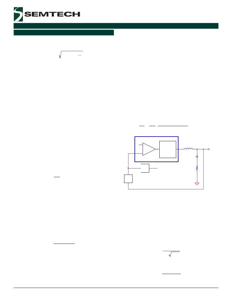
�Main� Control� Loop� Design�
�The� goal� of� compensation� is� to� shape� the� frequency�
�response� charatericstics� of� the� buck� converter� to�
�achieve� a� better� DC� accuracy� and� a� faster� transient�
�response� for� the� output� voltage,� while� maintaining�
�the� loop� stability.�
�The� block� diagram� in� Figure� 10� represents� the� control�
�loop� of� a� buck� converter� designed� with� the� SC2544.� The�
�control� loop� consists� of� a� compensator,� a� PWM� modula-�
�tor,� and� an� LC� filter.�
�The� LC� filter� and� PWM� modulator� represent� the� small�
�signal� model� of� the� buck� converter� operating� at� fixed�
�switching� frequency.� The� transfer� function� of� the�
�model� is� given� by:�
�V� 1� +� sR� ESR� C�
�Due� to� non-overlapping� conduction� between� the� top� and�
�the� bottom� MOSFET’s,� the� internal� body� diode� or� the�
�external� Schottky� diode� across� the� drain� and� source�
�terminals� always� conducts� prior� to� the� turn� on� of� the�
�V� O�
�V� C�
�=� IN� ?�
�V� m� 1� +� sL� /� R� +� s� 2� LC�
�bottom� MOSFET.� The� bottom� MOSFET� switches� on� with�
�only� a� diode� voltage� between� its� drain� and� source�
�REF�
�+�
�PWM�
�L�
�Vo�
�terminals.� The� switching� loss� is� negligible� due� to� near� zero-�
�voltage� switching.�
�The� gate� losses� are� estimated� as�
�R� g�
�P� bg� =�
�Q� g� V� cc� f� s� .�
�R� gt�
�REF�
�Zs�
�-�
�Zf�
�EA�
�MODULATOR�
�ERROUT�
�Co�
�Resr�
�The� total� bottom� switch� losses� are� then�
�T� j� ,� max� ?� T� a� ,� max�
�F� O� =�
�P� b� =P� bc� +P� bg� .�
�Once� the� power� losses� for� the� top� and� bottom�
�MOSFET� ’s� are� known,� thermal� and� package� design�
�at� component� and� system� level� should� be� done� to�
�verify� that� the� maximum� die� junction� temperature�
�(T� j,max� ,� usually� 125� o� C)� is� not� exceeded� under� the�
�worst-case� condition.� The� equivalent� thermal�
�impedance� from� junction� to� ambient� (� θ� ja� )� should�
�satisfy�
�θ� ja� ≤� .�
�P� loss�
�θ� ja� depends� on� the� die� to� substrate� bonding,�
�packaging� material,� the� thermal� contact� surface,�
�thermal� compound� property,� the� available� effective�
�Fig.� 10.� Block� diagram� of� the� control� loop.�
�where� V� IN� is� the� input� voltage,� Vm� is� the� amplitude� of�
�the� internal� ramp,� and� R� is� the� equivalent� load.�
�The� model� is� a� second� order� system� with� a� finite� DC�
�gain,� a� complex� pole� pair� at� Fo,� and� an� ESR� zero� at�
�Fz,� as� shown� in� Figure� 11.� The� locations� of� the� poles�
�and� zero� are� determined� by:�
�1�
�2� π� LC� O�
�heat� sink� area,� and� the� air� flow� condition� (natual� or�
�forced� convection).� Actual� temperature� measurement�
�of� the� prototype� should� be� carried� out� to� verify� the�
�thermal� design.�
�?� 2005� Semtech� Corp.�
�15�
�F� Z� =�
�1�
�2� π� R� e� sr� C� O�
�www.semtech.com�
�相关PDF资料 |
PDF描述 |
|---|---|
| SC2595MLTRT | IC DDR TERMINATION REG 16-MLPQ |
| SC2596STRT | IC INTEGRTD DDRII TERM REG 8SOIC |
| SC2608BSTRT | IC REG CTRLR BUCK PWM VM 8-SOIC |
| SC283WLTRT | IC REG BUCK SYNC ADJ 1.8A 18MLPQ |
| SC286ULTRT | IC REG BUCK SYNC ADJ 4A 28MLPQ |
相关代理商/技术参数 |
参数描述 |
|---|---|
| SC2545 | 制造商:SEMTECH 制造商全称:Semtech Corporation 功能描述:High Performance Wide Input Range Dual Synchronous Buck Controller |
| SC2545EVB | 制造商:SEMTECH 制造商全称:Semtech Corporation 功能描述:High Performance Wide Input Range Dual Synchronous Buck Controller |
| SC2545MLTRT | 制造商:Semtech Corporation 功能描述:Controller IC |
| SC2545TSTRT | 制造商:Semtech Corporation 功能描述:Controller IC 制造商:Semtech Corporation 功能描述:DC DC Cntrlr Dual-OUT Synchronous Buck Controller/PWM DC to DC Controller 4.5V to 28V Input 24-Pin TSSOP T/R |
| SC25-500VP | 制造商:JAMECO VALUEPRO 功能描述:CABLE,SHIELDED,25 CONDUCTOR,GRAY,24AWG,500 FEET,ROUND |
发布紧急采购,3分钟左右您将得到回复。