参数资料
| 型号: | SC410MLTRT |
| 厂商: | Semtech |
| 文件页数: | 13/26页 |
| 文件大小: | 0K |
| 描述: | IC REG BUCK SYNC ADJ 3A 10MLPD |
| 标准包装: | 1 |
| 系列: | EcoSpeed® |
| 类型: | 降压(降压) |
| 输出类型: | 可调式 |
| 输出数: | 1 |
| 输出电压: | 0.75 V ~ 7.5 V |
| 输入电压: | 5.5 V ~ 24 V |
| 频率 - 开关: | 200kHz ~ 1MHz |
| 电流 - 输出: | 3A |
| 同步整流器: | 是 |
| 工作温度: | -40°C ~ 85°C |
| 安装类型: | 表面贴装 |
| 封装/外壳: | 10-VFDFN 裸露焊盘 |
| 包装: | 标准包装 |
| 供应商设备封装: | 10-MLPD(3x3) |
| 其它名称: | SC410MLDKR |
�� �
�
�SC410�
�Applications� Information� (continued)�
�-�
�+�
�FB�
�Ref.�
�V� LX_FILTER�
�V� IN�
�PWM�
�S�
�R�
�One-Shot�
�Timer�
�Q�
�Hi-side�
�and�
�Lo-side�
�Gate�
�Drivers�
�V� IN�
�Q1�
�V� LX�
�Q2�
�LPF�
�L�
�ESR�
�C� OUT�
�+�
�V� LX_FILTER�
�V� OUT�
�FB�
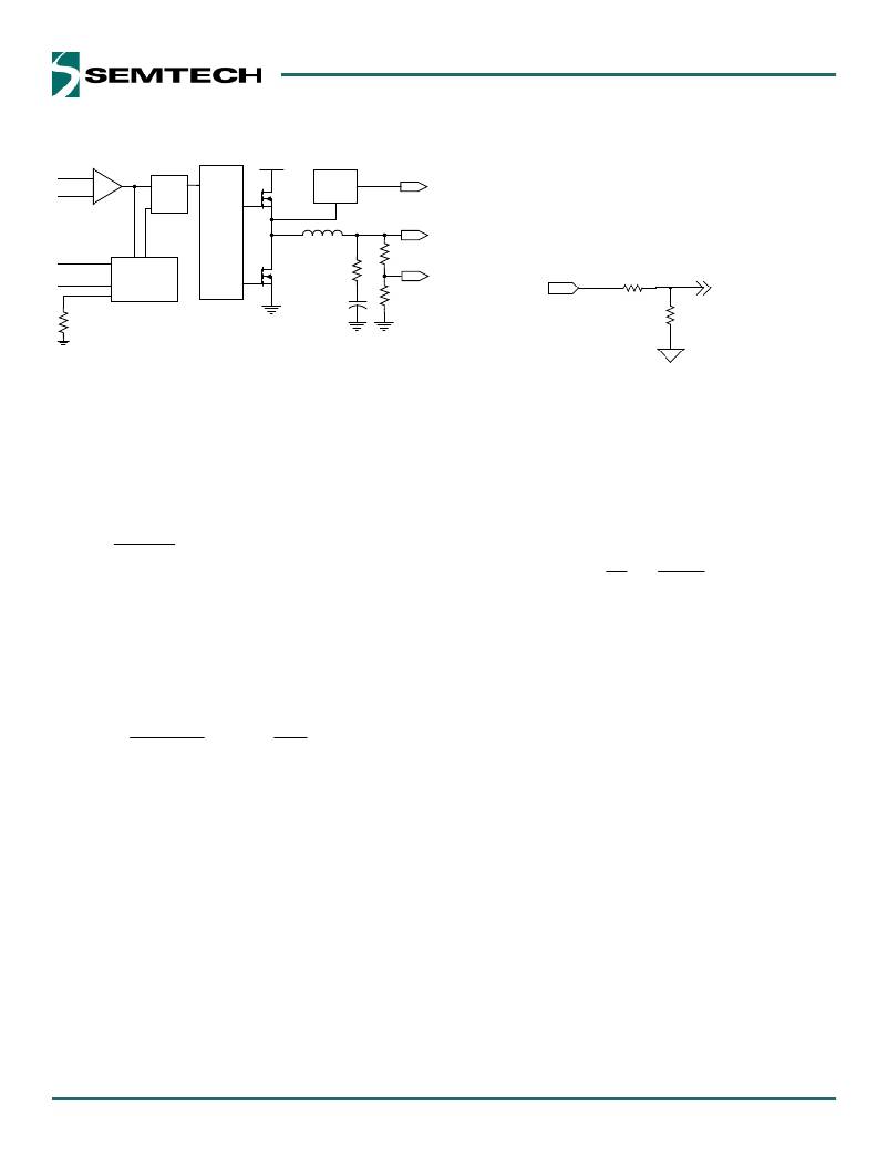
�V� OUT� Voltage� Selection�
�The� switcher� output� voltage� is� regulated� by� comparing�
�V� OUT� as� seen� through� a� resistor� divider� at� the� FB� pin� to� the�
�internal� 750mV� reference� voltage,� see� Figure� 3.�
�V� OUT� To� FB� pin�
�R� 1�
�R� 2�
�R� TON�
�Time� =� K� x� (V� OUT� /V� IN� )�
�Figure� 2� —� On-Time� Generation�
�f� SW�
�R� 1� V� RIPPLE�
�R� 2�
�V� OUT� 0� .� 75� 1�
�1� V� IN�
�25pF� f� SW�
�V� OUT�
�R� TON� _� MAX�
�?�
�?�
�Thismethodautomaticallyproducesanon-timethatis�
�proportional� to� V� OUT� and� inversely� proportional� to� V� IN� .�
�Under� steady-state� operating� conditions� in� continuous�
�conduction� mode,� the� switching� frequency� can� be� deter-�
�mined� from� the� on-time� by� the� following� equation.�
�V� OUT�
�t� ON� V� IN�
�The� SC410� uses� an� external� resistor� to� set� the� on-time�
�which� indirectly� sets� the� frequency.� The� on-time� can� be�
�programmed� to� provide� operating� frequencies� from�
�200kHz� to� 1MHz� using� a� resistor� between� the� TON� pin�
�and� ground.� The� resistor� value� is� selected� by� the� follow-�
�ing� equation.�
�R� TON� 400� 1� .� 2�
�The� maximum� R� TON� value� allowed� is� shown� by� the� follow-�
�ing� equation.�
�V� IN� _� MIN�
�10� 1� .� 5� A�
�Immediately� after� the� on-time,� the� DL� (the� drive�
�signal� for� the� low� side� FET)� output� drives� high� to�
�turn� on� the� low-side� MOSFET.� DL� has� a� minimum�
�high� time� of� ~320ns,� after� which� DL� continues� to�
�stay� high� until� one� of� the� following� occurs:�
�V� FB� falls� below� the� 750mV� reference�
�The� zero� cross� detector� senses� that� the� voltage�
�on� the� LX� node� is� below� ground.� PSAVE� is� acti-�
�Figure� 3� —� Output� Voltage� Selection�
�Note� that� this� control� method� regulates� the� valley� of� the�
�output� ripple� voltage,� not� the� DC� value.� The� DC� output�
�voltage� V� OUT� is� offset� by� the� output� ripple� according� to�
�the� following� equation.�
�2�
�Enable� Input�
�The� EN� input� is� used� to� enable� or� disable� the� switching�
�regulator.� When� EN� is� low� (grounded),� the� switching� regu-�
�lator� and� LDO� are� disabled� and� the� SC410� is� in� its� lowest�
�power� state.� When� disabled,� the� output� power� switches�
�are� tri-stated.� When� EN� is� higher� than� 0.8V,� the� internal�
�LDO� will� be� activated.� The� switching� regulator� remains� off�
�until� the� voltage� at� the� EN� pin� exceeds� 1.5V.�
�The� EN� pin� can� be� used� for� implementing� UVLO� for� the�
�input� voltage� by� configuring� a� voltage� divider� from� VIN� to�
�EN� to� PGND.�
�Continuous� Mode� Operation�
�The� SC410� operates� in� CCM� (Continuous� Conduction�
�Mode)� at� larger� load� currents� when� the� load� is� greater�
�than� or� equal� to� half� of� the� inductor� ripple� current� (Figure�
�4).� In� this� mode� one� of� the� power� MOSFETs� is� always� on,�
�with� no� intentional� dead� time� other� than� to� avoid� cross-�
�conduction.� This� mode� of� operation� results� in� uniform�
�frequency.�
�vated� 8� periods� after� the� zero� cross� is� detected.�
�13�
�相关PDF资料 |
PDF描述 |
|---|---|
| SC412AMLTRT | IC REG CTRLR BUCK PWM 16-MLP |
| SC419ULTRT | IC REG CTRLR BUCK PWM 20-MLPQ |
| SC4211STRT | IC REG LDO FIX/ADJ 1A 8-SOIC |
| SC4212MLTRT | IC REG LDO ADJ 1A 8MLPD |
| SC4215ASTRT | IC REG LDO FIX/ADJ 2A 8-SOIC |
相关代理商/技术参数 |
参数描述 |
|---|---|
| SC411 | 制造商:SEMTECH 制造商全称:Semtech Corporation 功能描述:Synchronous Buck Pseudo-Fixed Frequency Power Supply Controller |
| SC411201B | 制造商:Freescale Semiconductor 功能描述:MOTSC411201B ACCTON:110000000028H |
| SC411209B | 制造商:Freescale Semiconductor 功能描述: |
| SC411212C | 制造商:Freescale Semiconductor 功能描述: |
| SC411EVB | 制造商:SEMTECH 制造商全称:Semtech Corporation 功能描述:Synchronous Buck Pseudo-Fixed Frequency Power Supply Controller |
发布紧急采购,3分钟左右您将得到回复。