- 您现在的位置:买卖IC网 > PDF目录98079 > SDA20C440 (SIEMENS A G) 8-BIT, MROM, MICROCONTROLLER, PQFP80 PDF资料下载
参数资料
| 型号: | SDA20C440 |
| 厂商: | SIEMENS A G |
| 元件分类: | 微控制器/微处理器 |
| 英文描述: | 8-BIT, MROM, MICROCONTROLLER, PQFP80 |
| 封装: | PLASTIC, MQFP-80 |
| 文件页数: | 18/55页 |
| 文件大小: | 990K |
| 代理商: | SDA20C440 |
第1页第2页第3页第4页第5页第6页第7页第8页第9页第10页第11页第12页第13页第14页第15页第16页第17页当前第18页第19页第20页第21页第22页第23页第24页第25页第26页第27页第28页第29页第30页第31页第32页第33页第34页第35页第36页第37页第38页第39页第40页第41页第42页第43页第44页第45页第46页第47页第48页第49页第50页第51页第52页第53页第54页第55页
SDA 20C440
Semiconductor Group
25
Data Reception
In idle state the dataline on pin RXD is held at high level. The beginning of a data byte starts with
the first ‘1 – 0’ transition (start bit), which also synchronizes the baudrate generator. After this, eight
or nine data bits are read according to the selected mode with the clock of the baudrate generator.
In mode II the parity of the data byte is compared with the parity bit automatically. The stop bit is
always tested for the value ‘1’. If an error is detected, the appropriate error flag is set and causes an
interrupt, if enabled.
In case of no error, the received data byte is written into the register RXBUF and at the same time
the reception is signaled to the CPU using interrupt RXINT. If the data byte in the receive register
RXBUF is to be overwritten by a new data byte before the CPU has read this register, the overwrite
error flag is set and the control interrupt is activated.
Data Transmission
The transmission of a data word is started automatically by writing to the transmit register. The data
word of register TXBUF is loaded into the shift register TSREG. With the clock of the baudrate
generator the data value is shifted to pin TXD. The data word consists of an automatically generated
start bit, eight or nine data bits and one stop bit. In mode II the parity bit is computed and is
transmitted as the nineth data bit.
Transmit and Receive Register
The CPU writes the data to be sent into the transmit buffer TXBUF. It is a special function register
with write-only access. While reading from this address location, the receive register RXBUF will be
available.
Receive-Register
The SART-module writes the received data into the receive register RXBUF. It is a special-function-
register with ‘read-only’ access. While writing with this address the transmit register will be written.
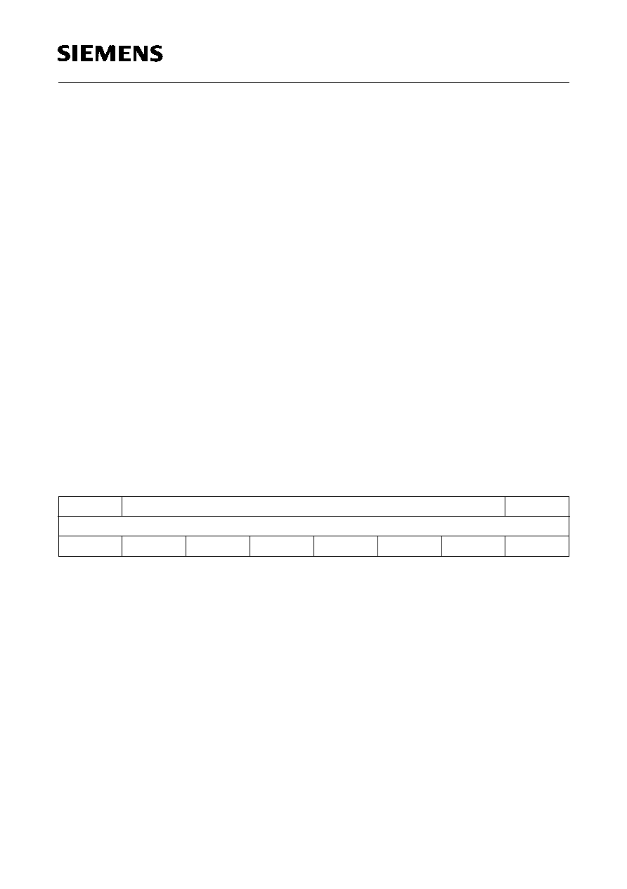
MSB
SFR-Address: C3H
LSB
SABUF: Serial Port Transmit/Receive Buffer
D7
D6
D5
D4
D3
D2
D1
D0
相关PDF资料 |
PDF描述 |
|---|---|
| SDA20C840 | 8-BIT, MROM, 4.5 MHz, MICROCONTROLLER, PQFP80 |
| SDC2200DUT3D | 1500 MHz, MICROPROCESSOR, CPGA453 |
| SDC2800DUT3D | 2000 MHz, MICROPROCESSOR, CPGA453 |
| SED1200F0B | 16 X 50 DOTS DOT MAT LCD DRVR AND DSPL CTLR, PQFP80 |
| SED1210F0A | 16 X 40 DOTS DOT MAT LCD DRVR AND DSPL CTLR, PQFP80 |
相关代理商/技术参数 |
参数描述 |
|---|---|
| SDA2101 | 制造商:INFINEON 制造商全称:Infineon Technologies AG 功能描述:FREQUENCY DIVIDER 1:64 |
| SDA2112-2 | 制造商:INFINEON 制造商全称:Infineon Technologies AG 功能描述:TV PLL FOR 125KHZ RESOLUTION |
| SDA2120 | 制造商:INFINEON 制造商全称:Infineon Technologies AG 功能描述:120 MHz PLL for AM/FM Receivers |
| SDA2121-2 | 制造商:INFINEON 制造商全称:Infineon Technologies AG 功能描述:PLL WITH I2C BUS FOR AM/FM RECEIVERS |
| SDA2121-2X | 制造商:INFINEON 制造商全称:Infineon Technologies AG 功能描述:PLL WITH I2C BUS FOR AM/FM RECEIVERS |
发布紧急采购,3分钟左右您将得到回复。