- 您现在的位置:买卖IC网 > PDF目录98079 > SED122ADXA 16 X 60 DOTS DOT MAT LCD DRVR AND DSPL CTLR, UUC165 PDF资料下载
参数资料
| 型号: | SED122ADXA |
| 元件分类: | 显示控制器 |
| 英文描述: | 16 X 60 DOTS DOT MAT LCD DRVR AND DSPL CTLR, UUC165 |
| 封装: | DIE-165 |
| 文件页数: | 3/50页 |
| 文件大小: | 398K |
| 代理商: | SED122ADXA |
第1页第2页当前第3页第4页第5页第6页第7页第8页第9页第10页第11页第12页第13页第14页第15页第16页第17页第18页第19页第20页第21页第22页第23页第24页第25页第26页第27页第28页第29页第30页第31页第32页第33页第34页第35页第36页第37页第38页第39页第40页第41页第42页第43页第44页第45页第46页第47页第48页第49页第50页
EPSON
4–11
SED1220
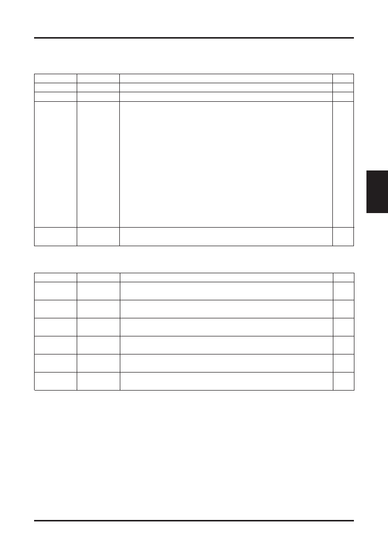
DESCRIPTION OF PINS
Power Pins
LCD Power Circuit Pins
Pin name
I/O
Description
Q’ty
VDD
Power supply Connected to logic supply. Common with MPU power terminal VCC.1
VSS
Power supply 0V power terminal connected to system ground.
1
V0, V1
Power supply Multi-level power supply for liquid crystal drive.
6
V2, V3
The voltage determined in the liquid crystal cell is resistance-
V4, V5
divided or impedance-converted by operational amplifier, and the
resultant voltage is applied.
The potential is determined on the basis of VDD and the following
equation must be respected.
VDD = V0
≥ V1 ≥ V2 ≥ V3 ≥ V4 ≥ V5
VDD
≥ VSS ≥ V5 ≥ VOUT
When the built-in power supply is ON, the following voltages are
given to pins V1 to V4 by built-in power circuit:
V1 = 1/5 V5
(1/4 V5)
V2 = 2/5 V5
(2/4 V5)
V3 = 3/5 V5
(3/4 V5)
V4 = 4/5 V5
(4/4 V5) voltage ratings in ( ) are for optinal choices.
VS1
O
Power supply voltage output pin for oscillating circuit, and DC/DC
1
source. Don’t connect this pin to an external load.
Pin name
I/O
Description
Q’ty
CAP1+
O
Capacitor positive side connecting pin for boosting.
1
This pin connects the capacitor with pin CAP1–.
CAP1–
O
Capacitor negative side connecting pin for boosting.
1
This pin connects a capacitor with pin CAP+.
CAP2+
O
Capacitor positive side connecting pin for boosting.
1
This pin connects a capacitor with pin CAP2–.
CAP2–
O
Capacitor negative side connecting pin for boosting.
1
This pin connects a capacitor with pin CAP2+.
VOUT
O
Output pin for boosting. This pin connects a smoothing capacitor
1
with VDD pin.
VR
I
Voltage regulating pin. This pin gives a voltage between VDD and
1
V5 by resistance-division of voltage.
相关PDF资料 |
PDF描述 |
|---|---|
| SED1278FOD | 16 X 40 DOTS DOT MAT LCD DRVR AND DSPL CTLR, PQFP80 |
| SED1278F | 16 X 40 DOTS DOT MAT LCD DSPL CTLR, PQFP80 |
| SED1330FBA | DOT MAT LCD DSPL CTLR, PQFP60 |
| SED1330FBB | 640 X 256 DOTS DOT MAT LCD DSPL CTLR, PQFP60 |
| SED1335FOA | DOT MAT LCD DSPL CTLR, PQFP60 |
相关代理商/技术参数 |
参数描述 |
|---|---|
| SED1278 | 制造商:未知厂家 制造商全称:未知厂家 功能描述:CMOS DOT MATRIX LCD CONTROLLER DRIVER |
| SED1278D | 制造商:EPSON 制造商全称:EPSON 功能描述:Dot Matrix LCD Controller Driver |
| SED1278D0A | 制造商:未知厂家 制造商全称:未知厂家 功能描述:CMOS DOT MATRIX LCD CONTROLLER DRIVER |
| SED1278D0B | 制造商:未知厂家 制造商全称:未知厂家 功能描述:CMOS DOT MATRIX LCD CONTROLLER DRIVER |
| SED1278D0C | 制造商:未知厂家 制造商全称:未知厂家 功能描述:CMOS DOT MATRIX LCD CONTROLLER DRIVER |
发布紧急采购,3分钟左右您将得到回复。