- 您现在的位置:买卖IC网 > PDF目录10910 > SI3056-D-FS (Silicon Laboratories Inc)IC SYSTEM-SIDE DAA 16SOIC PDF资料下载
参数资料
| 型号: | SI3056-D-FS |
| 厂商: | Silicon Laboratories Inc |
| 文件页数: | 30/94页 |
| 文件大小: | 0K |
| 描述: | IC SYSTEM-SIDE DAA 16SOIC |
| 标准包装: | 48 |
| 数据格式: | V.92 |
| 电源电压: | 3 V ~ 3.6 V |
| 安装类型: | 表面贴装 |
| 封装/外壳: | 16-SOIC(0.154",3.90mm 宽) |
| 供应商设备封装: | 16-SOIC N |
| 包装: | 管件 |
第1页第2页第3页第4页第5页第6页第7页第8页第9页第10页第11页第12页第13页第14页第15页第16页第17页第18页第19页第20页第21页第22页第23页第24页第25页第26页第27页第28页第29页当前第30页第31页第32页第33页第34页第35页第36页第37页第38页第39页第40页第41页第42页第43页第44页第45页第46页第47页第48页第49页第50页第51页第52页第53页第54页第55页第56页第57页第58页第59页第60页第61页第62页第63页第64页第65页第66页第67页第68页第69页第70页第71页第72页第73页第74页第75页第76页第77页第78页第79页第80页第81页第82页第83页第84页第85页第86页第87页第88页第89页第90页第91页第92页第93页第94页
Si3056
Si3018/19/10
36
Rev. 1.05
5.24. Filter Selection
The Si3056 supports additional filter selections for the
receive and transmit signals as defined in Table 11 and
Table 12 on page 15. The IIRE bit (Register 16, bit 4)
selects between the IIR and FIR filters. The IIR filter
provides a shorter, but non-linear, group delay
alternative to the default FIR filter and only operates
with an 8 kHz sample rate. Also, on the Si3019 line-side
device, the FILT bit (Register 31, bit 1) selects a –3 dB
low frequency pole of 5 Hz when cleared and 200 Hz
when set. The FILT bit affects the receive path only.
5.25. Clock Generation
The Si3056 has an on-chip clock generator. Using a
single MCLK input frequency, the Si3056 generates all
the desired standard modem sample rates.
The clock generator consists of two phase-locked loops
(PLL1 and PLL2) that achieve the desired sample
frequencies. Figure 26 illustrates the clock generator.
The architecture of the dual PLL scheme provides fast
lock time on initial start-up, fast lock time when
changing modem sample rates, high noise immunity,
and can change modem sample rates with a single
register write. Many MCLK frequencies between
1 and 60 MHz are supported. MCLK should be from a
clean source, preferably directly from a crystal with a
constant frequency and no dropped pulses.
In serial mode 2 (refer to the “5.26.Digital Interface”
section), the Si3056 operates as a slave device. The
clock generator is configured based on the SRC register
to generate the required internal clock frequencies. In
this mode, PLL2 is powered-down. For further details of
slave mode operation, see "5.27.Multiple Device
5.25.1. Programming the Clock Generator
As shown in Figure 26, PLL1 must output a clock equal
to 98.304 MHz (FBASE). The FBASE is determined by
programming the following registers:
Register 8: PLL1 N[7:0] divider.
Register 9: PLL1 M[7:0] divider.
The main design consideration is the generation of a
base frequency, defined as follows:
N (Register 8) and M (Register 9) are 8-bit unsigned
values. FMCLK is the frequency of the clock provided to
the MCLK pin.
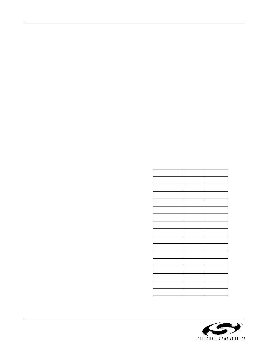
Table 20 lists several standard crystal oscillator rates
that can be supplied to MCLK. This list represents a
sample of MCLK frequency choices. Many others are
possible.
After PLL1 is programmed, the SRC[3:0] bits can
achieve the standard modem sampling rates with a
single write to Register 7. See "Register 7.Sample Rate
When programming the registers of the clock generator,
the order of register writes is important. For PLL1
updates, N (Register 8, bits 7:0) must be written first,
then immediately followed by a write to M (Register 9,
bits 7:0).
The values shown in Table 20 satisfy the preceding
equation. However, when programming the registers for
N and M, the value placed in these registers must be
one less than the value calculated from the equations.
For example, with an MCLK of 46.08 MHz, the values
placed in the N and M registers are 0x0Dh and 0x1Fh,
respectively.
FBASE
FMCLK M
×
N
-----------------------------
98.304 MHz
==
Table 20. MCLK Examples
MCLK (MHz)
N
M
1.8432
3
160
4.0960
1
24
6.1440
1
16
8.1920
1
12
9.2160
3
32
10.3680
27
256
11.0592
9
80
12.288
1
8
14.7456
3
20
18.4320
3
16
24.5760
1
4
25.8048
21
80
44.2368
9
20
46.0800
15
32
47.9232
39
80
56.0000
35
36
相关PDF资料 |
PDF描述 |
|---|---|
| PIC16C71/JW | IC MCU EPROM 1KX14 A/D 18CDIP |
| SI3018-F-FS-R | IC ISOMODEM LINE-SIDE DAA 16SOIC |
| VE-2N3-IX-F4 | CONVERTER MOD DC/DC 24V 75W |
| VE-2N3-IX-F3 | CONVERTER MOD DC/DC 24V 75W |
| DS2251T-64-16# | IC MCU 64KB 16MHZ 72-SIMM |
相关代理商/技术参数 |
参数描述 |
|---|---|
| SI3056-D-FSR | 功能描述:电信线路管理 IC Si3056 DAA System Side SSI Interface RoHS:否 制造商:STMicroelectronics 产品:PHY 接口类型:UART 电源电压-最大:18 V 电源电压-最小:8 V 电源电流:30 mA 最大工作温度:+ 85 C 最小工作温度:- 40 C 安装风格:SMD/SMT 封装 / 箱体:VFQFPN-48 封装:Tray |
| SI3056-D-ZS3R | 制造商:Silicon Laboratories Inc 功能描述:MODEM CHIP CHIPSET 56KBPS - Tape and Reel |
| SI3056-F-FS | 制造商:Silicon Laboratories Inc 功能描述: |
| SI3056-FS | 功能描述:IC SYSTEM-SIDE DAA 16SOIC RoHS:是 类别:集成电路 (IC) >> 接口 - 调制解调器 - IC 和模块 系列:- 标准包装:25 系列:- 数据格式:V.21,V.22,V.23,V.29,V.32,V.34,V.90,V.92,Bell 103,Bell 212A 波特率:33.6k 电源电压:3.3V 安装类型:- 封装/外壳:- 供应商设备封装:- 包装:托盘 配用:591-1013-ND - KIT DEV SOCKETMODEM PARALLEL591-1009-ND - KIT DEV SRL SOCKETMODEM UNIVERSL 其它名称:MT5656SMI-P-V-34.R2-SPMT5656SMI-P-V-34.R2-SP-NDQ4711574 |
| SI3056-FSR | 制造商:Silicon Laboratories Inc 功能描述:SI3056 DAA SYSTEM-SIDE, SSI INTERFACE - LEAD-FREE SOIC 0 TO - Tape and Reel |
发布紧急采购,3分钟左右您将得到回复。