- 您现在的位置:买卖IC网 > PDF目录20504 > SI3402ISO-EVB (Silicon Laboratories Inc)BOARD EVAL POE ISOL FOR SI3402 PDF资料下载
参数资料
| 型号: | SI3402ISO-EVB |
| 厂商: | Silicon Laboratories Inc |
| 文件页数: | 12/22页 |
| 文件大小: | 0K |
| 描述: | BOARD EVAL POE ISOL FOR SI3402 |
| 标准包装: | 1 |
| 主要目的: | 特殊用途 DC/DC,以太网供电(POE) |
| 输出及类型: | 1,隔离 |
| 输出电压: | 5V |
| 输入电压: | 44 ~ 57 V |
| 稳压器拓扑结构: | 回扫 |
| 频率 - 开关: | 350kHz |
| 板类型: | 完全填充 |
| 已供物品: | 板,CD |
| 已用 IC / 零件: | Si3402 |
| 其它名称: | 336-1828 |
�� �
�
�Si3402�
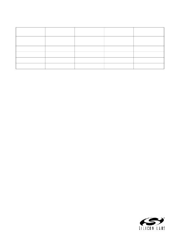
�Table� 10.� Class� Resistor� Values�
�Class�
�Usage�
�Peak� Power� Levels�
�Nominal� Class�
�RCL� Resistor� (1%,�
�Current�
�1/16� W)�
�0�
�Default�
�0.44� to� 12.95� W�
�<� 4� mA�
�>� 1.33� k� ?�
�(or� open� circuit)�
�1�
�2�
�3�
�4�
�Optional�
�Optional�
�Optional�
�PoE+�
�0.44� to� 3.84� W�
�3.84� to� 6.49� W�
�6.49� to� 12.95� W�
�12.95� to� 17� W�
�10.5� mA�
�18.5� mA�
�28� mA�
�40� mA�
�127� ?�
�69.8� ?�
�45.3� ?�
�30.9� ?�
�The� 802.3� specification� limits� the� classification� time� to�
�75� ms� to� limit� the� power� dissipated� in� the� PD.� If� the� PSE�
�classification� period� exceeds� 75� ms� and� the� die�
�temperature� rises� above� the� thermal� shutdown� limits,�
�the� thermal� protection� circuit� will� engage� and� disable�
�the� classification� current� source� in� order� to� protect� the�
�Si3402.� The� Si3402� stays� in� classification� mode� until�
�the� input� voltage� exceeds� 22� V� (the� upper� end� of� its�
�classification� operation� region).�
�3.2.4.� Under� Voltage� Lockout�
�The� 802.3� standard� specifies� the� PD� to� turn� on� when�
�the� line� voltage� rises� to� 42� V� and� for� the� PD� to� turn� off�
�when� the� line� voltage� falls� to� 30� V.� The� PD� must� also�
�maintain� a� large� on-off� hysteresis� region� to� prevent�
�wiring� losses� between� the� PSE� and� the� PD� from�
�causing� startup� oscillation.�
�The� Si3402� incorporates� an� undervoltage� lockout�
�(UVLO)� circuit� to� monitor� the� line� voltage� and� determine�
�when� to� apply� power� to� the� integrated� switching�
�regulator.� Before� the� power� is� applied� to� the� switching�
�regulator,� the� hotswap� switch� output� (HSO)� pin� is� high-�
�impedance� and� typically� follows� VPOS� as� the� input� is�
�ramped� (due� to� the� discharged� switcher� supply�
�capacitor).� When� the� input� voltage� rises� above� the�
�UVLO� turn-on� threshold,� the� Si3402� begins� to� turn� on�
�the� internal� hotswap� power� MOSFET.� The� switcher�
�supply� capacitor� begins� to� charge� up� under� the� current�
�limit� control� of� the� Si3402,� and� the� HSO� pin� transitions�
�from� VPOS� to� VNEG.� The� Si3402� includes� hysteretic�
�UVLO� circuits� to� maintain� power� to� the� load� until� the�
�input� voltage� falls� below� the� UVLO� turn-off� threshold.�
�Once� the� input� voltage� falls� below� 30� V,� the� internal�
�hotswap� MOSFET� is� turned� off.�
�3.2.5.� Dual� Current� Limit� and� Switcher� Turn-On�
�The� Si3402� implements� dual� current� limits.� While� the�
�hotswap� MOSFET� is� charging� the� switcher� supply�
�capacitor,� the� Si3402� maintains� a� low� current� limit.� The�
�switching� regulator� is� disabled� until� the� voltage� across�
�the� hotswap� MOSFET� becomes� sufficiently� low,�
�indicating� the� switcher� supply� capacitor� is� almost�
�completely� charged.� When� this� threshold� is� reached,�
�the� switcher� is� activated,� and� the� hotswap� current� limit�
�is� increased.� This� threshold� also� has� hysteresis� to�
�prevent� systemic� oscillation� as� the� switcher� begins� to�
�draw� current� and� the� current� limit� is� increased,� which�
�allows� resistive� losses� in� the� cable� to� effectively�
�decrease� the� input� supply.�
�The� Si3402� stays� in� a� high-level� current� limit� mode� until�
�the� input� voltage� drops� below� the� UVLO� turn-off�
�threshold� or� excessive� power� is� dissipated� in� the�
�hotswap� switch.� This� dual� level� current� limit� allows� the�
�system� designer� to� design� powered� devices� for� use� with�
�both� legacy� and� compliant� PoE� systems.�
�An� additional� feature� of� the� dual� current� limit� circuitry� is�
�foldback� current� limiting� in� the� event� of� a� fault� condition.�
�When� the� current� limit� is� switched� to� the� higher� level,�
�400� mA� of� current� can� be� drawn� by� the� PD.� Should� a�
�fault� cause� more� than� this� current� to� be� consumed,� the�
�voltage� across� the� hotswap� MOSFET� will� increase� to�
�clamp� the� maximum� amount� of� power� consumed.� The�
�power� dissipated� by� the� MOSFET� can� be� very� high�
�under� this� condition.� If� the� fault� is� very� low� impedance,�
�the� voltage� across� the� hotswap� MOSFET� will� continue�
�to� rise� until� the� lower� current� limit� level� is� engaged,�
�further� reducing� the� dissipated� power.� If� the� fault�
�condition� remains,� the� thermal� overload� protection�
�circuitry� will� eventually� engage� and� shut� down� the�
�hotswap� interface� and� switching� regulator.� The� foldback�
�current� limiting� occurs� much� faster� than� the� thermal�
�overload� protection� and� is,� therefore,� necessary� for�
�comprehensive� protection� of� the� hotswap� MOSFET.�
�12�
�Rev.� 1.31�
�相关PDF资料 |
PDF描述 |
|---|---|
| MBR3050PT | DIODE SCHOTTKY 30A 50V TO-247AD |
| T95D277M004LZSS | CAP TANT 270UF 4V 20% 2917 |
| VI-23Z-CV-S | CONVERTER MOD DC/DC 2V 60W |
| IRDC3856 | BOARD EVAL FOR IR3856 |
| IRDC3839 | KIT EVAL REG 6A SUPIRBUCK DC/DC |
相关代理商/技术参数 |
参数描述 |
|---|---|
| SI3403-A-GM | 制造商:Silicon Laboratories Inc 功能描述:POE POWERED DEVICE (UP TO 17W, LOW-EMI) - RECOMMENDED FOR AL - Trays 制造商:Silicon Laboratories Inc 功能描述:IC POE CTLR TO 17W LOW EMI 20QFN 制造商:Silicon Laboratories Inc 功能描述:PoE Powered Device (up to 17W, low-EMI) |
| Si3403-A-GMR | 制造商:Silicon Laboratories Inc 功能描述:POE POWERED DEVICE (UP TO 17W, LOW-EMI) - RECOMMENDED FOR AL - Tape and Reel 制造商:Silicon Laboratories Inc 功能描述:PoE Powered Device (up to 17W, low-EMI) |
| SI3403DV-T1-E3 | 功能描述:MOSFET 20V 5.0A 3.2W RoHS:否 制造商:STMicroelectronics 晶体管极性:N-Channel 汲极/源极击穿电压:650 V 闸/源击穿电压:25 V 漏极连续电流:130 A 电阻汲极/源极 RDS(导通):0.014 Ohms 配置:Single 最大工作温度: 安装风格:Through Hole 封装 / 箱体:Max247 封装:Tube |
| SI3403DV-T1-GE3 | 功能描述:MOSFET 20V 5.0A 3.2W 70mohm @ 4.5V RoHS:否 制造商:STMicroelectronics 晶体管极性:N-Channel 汲极/源极击穿电压:650 V 闸/源击穿电压:25 V 漏极连续电流:130 A 电阻汲极/源极 RDS(导通):0.014 Ohms 配置:Single 最大工作温度: 安装风格:Through Hole 封装 / 箱体:Max247 封装:Tube |
| SI3407DV | 制造商:VISHAY 制造商全称:Vishay Siliconix 功能描述:P-Channel 20-V (D-S) MOSFET |
发布紧急采购,3分钟左右您将得到回复。