- 您现在的位置:买卖IC网 > PDF目录98081 > SIO10N268-NU (STANDARD MICROSYSTEMS CORP) MULTIFUNCTION PERIPHERAL, PQFP128 PDF资料下载
参数资料
| 型号: | SIO10N268-NU |
| 厂商: | STANDARD MICROSYSTEMS CORP |
| 元件分类: | 外设及接口 |
| 英文描述: | MULTIFUNCTION PERIPHERAL, PQFP128 |
| 封装: | 14 X 14 MM, 1MM THICKNESS, GREEN, TQFP-128 |
| 文件页数: | 198/251页 |
| 文件大小: | 1384K |
| 代理商: | SIO10N268-NU |
第1页第2页第3页第4页第5页第6页第7页第8页第9页第10页第11页第12页第13页第14页第15页第16页第17页第18页第19页第20页第21页第22页第23页第24页第25页第26页第27页第28页第29页第30页第31页第32页第33页第34页第35页第36页第37页第38页第39页第40页第41页第42页第43页第44页第45页第46页第47页第48页第49页第50页第51页第52页第53页第54页第55页第56页第57页第58页第59页第60页第61页第62页第63页第64页第65页第66页第67页第68页第69页第70页第71页第72页第73页第74页第75页第76页第77页第78页第79页第80页第81页第82页第83页第84页第85页第86页第87页第88页第89页第90页第91页第92页第93页第94页第95页第96页第97页第98页第99页第100页第101页第102页第103页第104页第105页第106页第107页第108页第109页第110页第111页第112页第113页第114页第115页第116页第117页第118页第119页第120页第121页第122页第123页第124页第125页第126页第127页第128页第129页第130页第131页第132页第133页第134页第135页第136页第137页第138页第139页第140页第141页第142页第143页第144页第145页第146页第147页第148页第149页第150页第151页第152页第153页第154页第155页第156页第157页第158页第159页第160页第161页第162页第163页第164页第165页第166页第167页第168页第169页第170页第171页第172页第173页第174页第175页第176页第177页第178页第179页第180页第181页第182页第183页第184页第185页第186页第187页第188页第189页第190页第191页第192页第193页第194页第195页第196页第197页当前第198页第199页第200页第201页第202页第203页第204页第205页第206页第207页第208页第209页第210页第211页第212页第213页第214页第215页第216页第217页第218页第219页第220页第221页第222页第223页第224页第225页第226页第227页第228页第229页第230页第231页第232页第233页第234页第235页第236页第237页第238页第239页第240页第241页第242页第243页第244页第245页第246页第247页第248页第249页第250页第251页
Advanced Notebook I/O for ISA or LPC Designs
Datasheet
Rev. 0.5 (03-24-05)
Page 50
SMSC SIO10N268
DATASHEET
The X-Bus supports flash speed selection by offering a programmable read/write pulse width (see section
12.4.3 X-Bus Memory Cycle Timing on page 230. The read/write pulse width is determined by the Pulse
Width Selection bits located in X-Bus Chip Select 0 Register at offset CR53. These bits allow the
read/write strobe to be held active for a minimum of 60, 90, 120, or 150 nsec.
The X-Bus Chips Select 0 Register offers a write protect bit. This bit affords the BIOS the ability to
program CR53 for a particular configuration, which cannot be altered until a VCC POR or Hard Reset.
NOTE:
To tristate the X-Bus for production line Flash update put the device in XNOR chain test mode.
8.6
ISA Interface (ISA Mode Only)
ISA Mode is enabled by pulling pin 54 (LPC_ISA) directly to VCC – a pull-up resistor should not be used.
The ISA interface is a standard AT (Advanced Technology) interface, that is compatible with the ISA
(Industry Standard Architecture) as documented by IEEE (IEEE P996 compatible). This interface supports
I/O and DMA transactions as defined by this defacto standard. In addition this interface has been modified
to have the option of supporting ISA devices that do not have an AEN output signal (Devices like the Intel
440MX chipset). The following sections define the signals on the ISA interface and the modifications made
to support special chipsets like the 440MX.
NOTE:
For ISA timing see section 12.5 Host Timing (ISA Mode Only) on page 232.
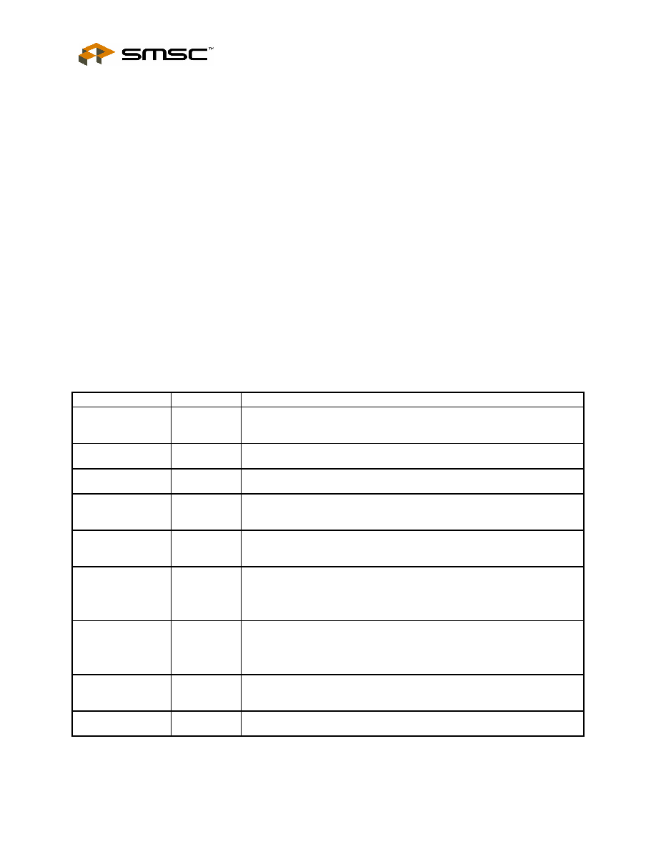
Table 8.6 - Description of ISA Signals
NAME
SYMBOL
DESCRIPTION
System Data Bus 0-7 SD0-SD7
The system data bus connection used by the host microprocessor to transmit
data to and from the chip. These pins are in a high-impedance state when not in
the output mode.
I/O Read
nIORD
This active low signal is issued by the host microprocessor to indicate an I/O
read operation.
I/O Write
nIOWR
This active low signal is issued by the host microprocessor to indicate an I/O
write operation.
Address Enable
AEN
Active high Address Enable indicates DMA operations on the host data bus.
Used internally to qualify appropriate address decodes. (See section 8.6.1 AEN
signal following table.)
System Address Bus
SA0-SA15
These host address bits determine the I/O address to be accessed during nIOR
and nIOW cycles. These bits are latched internally by the leading edge of nIOR
and nIOW. All internal address decodes use the full A0 to A15 address bits.
DMA Request
0, 1, 2, 3
DRQ_0
DRQ_1
DRQ_2
DRQ_3
These active high outputs are the DMA request for byte transfers of data
between the host and the chip. These signals are cleared on the last byte of the
data transfer by the nDACK signal going low (or by nIOR going low if nDACK
was already low as in demand mode).
nDMA
Acknowl-edge
0, 1, 2, 3
nDACK_0
nDACK_1
nDACK_2
nDACK_3
These are active low inputs acknowledging the request for a DMA transfer of
data between the host and the chip. These inputs enable the DMA read or write
internally.
Terminal Count
TC
This signal indicates that DMA data transfer is complete. TC is only accepted
when nDACK_x is low. In AT and PS/2 model 30 modes, TC is active high and
in PS/2 mode, TC is active low.
Serial IRQ
SER_IRQ
Serial IRQ pin used with the PCI_CLK pin to transfer SIO10N268 interrupts to
the host.
相关PDF资料 |
PDF描述 |
|---|---|
| SIS300 | GRAPHICS PROCESSOR, PBGA365 |
| SK12430PJT | 800 MHz, OTHER CLOCK GENERATOR, PQCC28 |
| SK12439PJ | 800 MHz, OTHER CLOCK GENERATOR, PQCC28 |
| SK12439PJT | 800 MHz, OTHER CLOCK GENERATOR, PQCC28 |
| SL15100ZIT-XXX | 200 MHz, OTHER CLOCK GENERATOR, PDSO8 |
相关代理商/技术参数 |
参数描述 |
|---|---|
| SIO665GT | 功能描述:界面开发工具 Evaluation Board RoHS:否 制造商:Bourns 产品:Evaluation Boards 类型:RS-485 工具用于评估:ADM3485E 接口类型:RS-485 工作电源电压:3.3 V |
| SIO666GT | 功能描述:界面开发工具 Evaluation Board RoHS:否 制造商:Bourns 产品:Evaluation Boards 类型:RS-485 工具用于评估:ADM3485E 接口类型:RS-485 工作电源电压:3.3 V |
| SIO669 | 功能描述:界面开发工具 Evaluation Board RoHS:否 制造商:Bourns 产品:Evaluation Boards 类型:RS-485 工具用于评估:ADM3485E 接口类型:RS-485 工作电源电压:3.3 V |
| SIOLS1000V2 | 制造商:SECELECTRONICS 制造商全称:SECELECTRONICS 功能描述:Current Sensors |
| SIOLS2000V2 | 制造商:SECELECTRONICS 制造商全称:SECELECTRONICS 功能描述:Current Sensors |
发布紧急采购,3分钟左右您将得到回复。