- 您现在的位置:买卖IC网 > PDF目录98083 > SM320VC33HFGM150 (TEXAS INSTRUMENTS INC) 32-BIT, 75 MHz, OTHER DSP, CQFP164 PDF资料下载
参数资料
| 型号: | SM320VC33HFGM150 |
| 厂商: | TEXAS INSTRUMENTS INC |
| 元件分类: | 数字信号处理 |
| 英文描述: | 32-BIT, 75 MHz, OTHER DSP, CQFP164 |
| 封装: | NCTB, CERAMIC, MO-113AA, QFP-164 |
| 文件页数: | 4/56页 |
| 文件大小: | 669K |
| 代理商: | SM320VC33HFGM150 |
第1页第2页第3页当前第4页第5页第6页第7页第8页第9页第10页第11页第12页第13页第14页第15页第16页第17页第18页第19页第20页第21页第22页第23页第24页第25页第26页第27页第28页第29页第30页第31页第32页第33页第34页第35页第36页第37页第38页第39页第40页第41页第42页第43页第44页第45页第46页第47页第48页第49页第50页第51页第52页第53页第54页第55页第56页
SM320VC33, SMJ320VC33
DIGITAL SIGNAL PROCESSOR
SGUS034E - FEBRUARY 2001 - REVISED OCTOBER 2002
12
POST OFFICE BOX 1443
HOUSTON, TEXAS 77251-1443
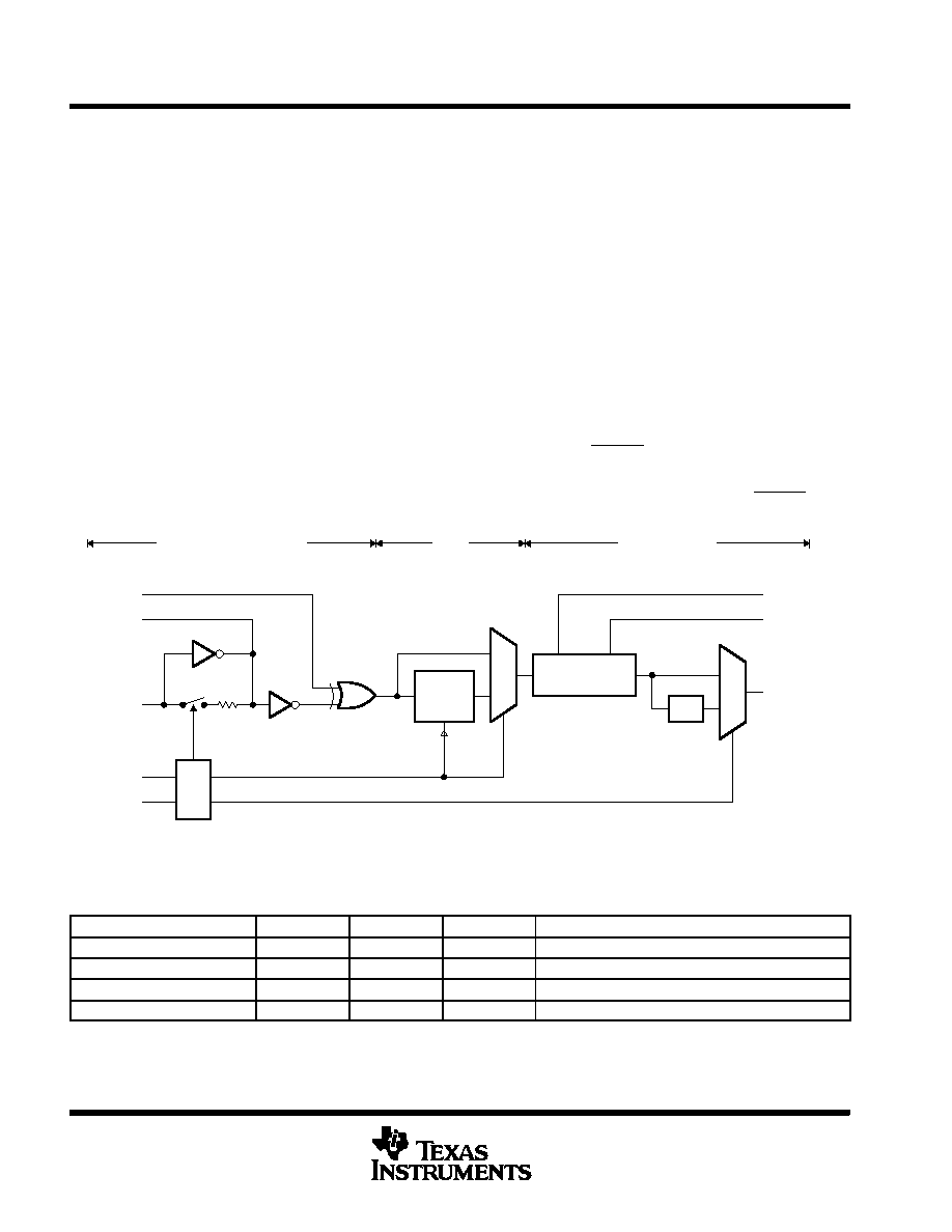
PLL and clock oscillator control
The clock mode control pins are decoded into four operational modes as shown in Figure 4. These modes
control clock divide ratios, oscillator, and PLL power (see Table 2).
When an external clock input or crystal is connected, the opposite unused input is simply grounded. An XOR
gate then passes one of the two signal sources to the PLL stage. This allows the direct injection of a clock
reference into EXTCLK, or 1-20 MHz crystals and ceramic resonators with the oscillator circuit. The two clock
sources include:
D A crystal oscillator circuit, where a crystal or ceramic resonator is connected across the XOUT and XIN pins
and EXTCLK is grounded.
D An external clock input, where an external clock source is directly connected to the EXTCLK pin, and XOUT
is left unconnected and XIN is grounded.
When the PLL is initially started, it enters a transitional mode during which the PLL acquires lock with the input
signal. Once the PLL is locked, it continues to track and maintain synchronization with the input signal. The PLL
is a simple x5 reference multiplier with bypass and power control.
The clock divider, under CPU control, reduces the clock reference by 1 (MAXSPEED), 1/16 (LOWPOWER), or
clock stop (IDLE2). Wake-up from the IDLE2 state is accomplished by a RESET or interrupt pin logic-low state.
A divide-by-two TMS320C31 equivalent mode of operation is also provided. In this case, the clock output
reference is further divided by two with clock synchronization being determined by the timing of RESET falling
relative to the present H1/H3 state.
Clock Divider
PLL
Clock & Crystal OSC
CLKMD1
CLKMD0
PLL PWR and Bypass
Oscillator Enable
C31 DIV2 Mode
LOWPOWER
MAXSPEED/
IDLE2
CPU CLOCK
1/2
U
M
X
X1, 1/16, Off
XOR
SEL
X
U
M
PLL
X5
EXTCLK
XIN
XOUT
RF
S1
Figure 4. Clock Generation
Table 2. Clock Mode Select Pins
CLKMD0
CLKMD1
FEEDBACK
PLLPWR
RATIO
NOTES
0
Off
1
Fully static, very low power
0
1
On
Off
1/2
Oscillator enabled
1
0
On
Off
1
Oscillator enabled
1
On
5
2 mA @ 60 MHz, 1.8 V PLL power. Oscillator enabled
相关PDF资料 |
PDF描述 |
|---|---|
| SM34020AHTM32 | GRAPHICS PROCESSOR, CQFP132 |
| SM563 | 4-BIT, MROM, MICROCONTROLLER, PQFP64 |
| SM565 | 4-BIT, MROM, MICROCONTROLLER, PQFP100 |
| SM5K7 | 4-BIT, MROM, MICROCONTROLLER |
| SM5L3 | 4-BIT, MROM, MICROCONTROLLER, PQFP80 |
相关代理商/技术参数 |
参数描述 |
|---|---|
| SM320VC33PGEA120EP | 功能描述:数字信号处理器和控制器 - DSP, DSC EP Dig Signal Proc RoHS:否 制造商:Microchip Technology 核心:dsPIC 数据总线宽度:16 bit 程序存储器大小:16 KB 数据 RAM 大小:2 KB 最大时钟频率:40 MHz 可编程输入/输出端数量:35 定时器数量:3 设备每秒兆指令数:50 MIPs 工作电源电压:3.3 V 最大工作温度:+ 85 C 封装 / 箱体:TQFP-44 安装风格:SMD/SMT |
| SM320VC5409-EP | 制造商:TI 制造商全称:Texas Instruments 功能描述:FIXED-POINT DIGITAL SIGNAL PROCESSOR |
| SM320VC5409GGU10EP | 功能描述:数字信号处理器和控制器 - DSP, DSC Fxd-pt Dig Sig Proc Mil enhanced RoHS:否 制造商:Microchip Technology 核心:dsPIC 数据总线宽度:16 bit 程序存储器大小:16 KB 数据 RAM 大小:2 KB 最大时钟频率:40 MHz 可编程输入/输出端数量:35 定时器数量:3 设备每秒兆指令数:50 MIPs 工作电源电压:3.3 V 最大工作温度:+ 85 C 封装 / 箱体:TQFP-44 安装风格:SMD/SMT |
| SM320VC5416-EP | 制造商:TI 制造商全称:Texas Instruments 功能描述:SM320VC5416-EP Fixed-Point Digital Signal Processor |
| SM320VC5416GGU16EP | 功能描述:数字信号处理器和控制器 - DSP, DSC Fxd-pt Dig Sig Proc Mil enhanced RoHS:否 制造商:Microchip Technology 核心:dsPIC 数据总线宽度:16 bit 程序存储器大小:16 KB 数据 RAM 大小:2 KB 最大时钟频率:40 MHz 可编程输入/输出端数量:35 定时器数量:3 设备每秒兆指令数:50 MIPs 工作电源电压:3.3 V 最大工作温度:+ 85 C 封装 / 箱体:TQFP-44 安装风格:SMD/SMT |
发布紧急采购,3分钟左右您将得到回复。