- 您现在的位置:买卖IC网 > PDF目录98083 > SM320VC33HFGM150 (TEXAS INSTRUMENTS INC) 32-BIT, 75 MHz, OTHER DSP, CQFP164 PDF资料下载
参数资料
| 型号: | SM320VC33HFGM150 |
| 厂商: | TEXAS INSTRUMENTS INC |
| 元件分类: | 数字信号处理 |
| 英文描述: | 32-BIT, 75 MHz, OTHER DSP, CQFP164 |
| 封装: | NCTB, CERAMIC, MO-113AA, QFP-164 |
| 文件页数: | 53/56页 |
| 文件大小: | 669K |
| 代理商: | SM320VC33HFGM150 |
第1页第2页第3页第4页第5页第6页第7页第8页第9页第10页第11页第12页第13页第14页第15页第16页第17页第18页第19页第20页第21页第22页第23页第24页第25页第26页第27页第28页第29页第30页第31页第32页第33页第34页第35页第36页第37页第38页第39页第40页第41页第42页第43页第44页第45页第46页第47页第48页第49页第50页第51页第52页当前第53页第54页第55页第56页
SM320VC33, SMJ320VC33
DIGITAL SIGNAL PROCESSOR
SGUS034E - FEBRUARY 2001 - REVISED OCTOBER 2002
6
POST OFFICE BOX 1443
HOUSTON, TEXAS 77251-1443
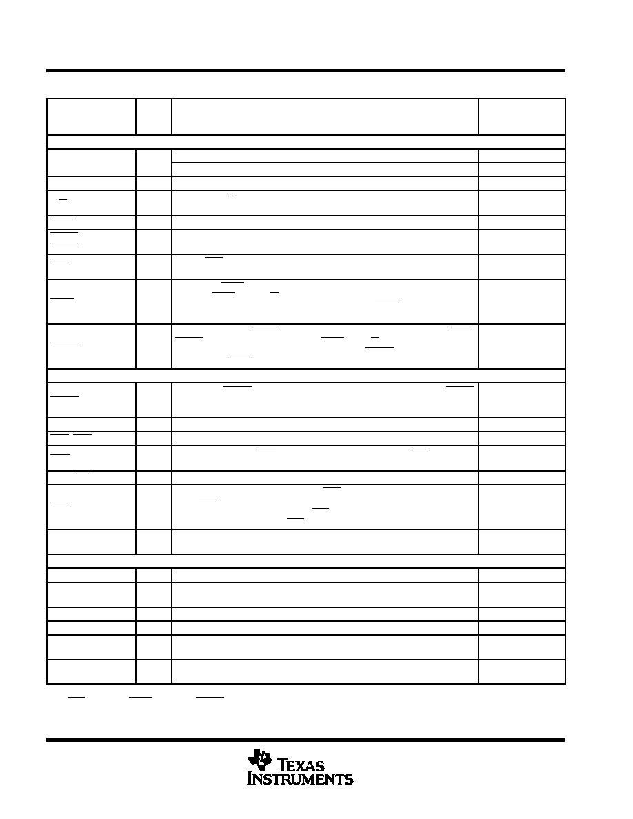
Terminal Functions
TERMINAL
TYPE
DESCRIPTION
CONDITIONS
WHEN
NAME
QTY
TYPE
DESCRIPTION
WHEN
SIGNAL IS Z TYPE
PRIMARY-BUS INTERFACE
D31 D0
32
I/O/Z
32-bit data port
S
H
R
D31- D0
32
I/O/Z
Data port bus keepers. (See Figure 9)
S
A23- A0
24
O/Z
24-bit address port
S
H
R
R/W
1
O/Z
Read/write. R/W is high when a read is performed and low when a write is performed
over the parallel interface.
S
H
R
STRB
1
O/Z
Strobe. For all external-accesses
S
H
PAGE0 -
PAGE3
1
O/Z
Page strobes. Four decoded page strobes for external access
S
H
R
RDY
1
I
Ready. RDY indicates that the external device is prepared for a transaction
completion.
HOLD
1
I
Hold. When HOLD is a logic low, any ongoing transaction is completed. A23- A0,
D31-D0, STRB, and R/W are placed in the high-impedance state and all
transactions over the primary-bus interface are held until HOLD becomes a logic high
or until the NOHOLD bit of the primary-bus-control register is set.
HOLDA
1
O/Z
Hold acknowledge. HOLDA is generated in response to a logic-low on HOLD.
HOLDA indicates that A23-A0, D31-D0, STRB, and R/W are in the high-impedance
state and that all transactions over the bus are held. HOLDA is high in response to
a logic-high of HOLD or the NOHOLD bit of the primary-bus-control register is set.
S
CONTROL SIGNALS
RESET
1
I
Reset. When RESET is a logic low, the device is in the reset condition. When RESET
becomes a logic high, execution begins from the location specified by the reset vec-
tor.
EDGEMODE
1
I
Edge mode. Enables interrupt edge mode detection.
INT3- INT0
4
I
External interrupts
IACK
1
O/Z
Internal acknowledge. IACK is generated by the IACK instruction. IACK can be used
to indicate when a section of code is being executed.
S
MCBL/MP
1
I
Microcomputer Bootloader/microprocessor mode-select
SHZ
1
I
Shutdown high impedance. When active, SHZ places all pins in the high-impedance
state. SHZ can be used for board-level testing or to ensure that no dual-drive
conditions occur. CAUTION: A low on SHZ corrupts the device memory and register
contents. Reset the device with SHZ high to restore it to a known operating condition.
XF1, XF0
2
I/O/Z
External flags. XF1 and XF0 are used as general-purpose I/Os or to support
interlocked processor instruction.
S
R
SERIAL PORT 0 SIGNALS
CLKR0
1
I/O/Z
Serial port 0 receive clock. CLKR0 is the serial shift clock for the serial port 0 receiver.
S
R
CLKX0
1
I/O/Z
Serial port 0 transmit clock. CLKX0 is the serial shift clock for the serial port 0
transmitter.
S
R
DR0
1
I/O/Z
Data-receive. Serial port 0 receives serial data on DR0.
S
R
DX0
1
I/O/Z
Data-transmit output. Serial port 0 transmits serial data on DX0.
S
R
FSR0
1
I/O/Z
Frame-synchronization pulse for receive. The FSR0 pulse initiates the data-receive
process using DR0.
S
R
FSX0
1
I/O/Z
Frame-synchronization pulse for transmit. The FSX0 pulse initiates the data-transmit
process using DX0.
S
R
I = input, O = output, Z = high-impedance state
S = SHZ active, H = HOLD active, R = RESET active
§ Recommended decoupling. Four 0.1
F for CVDD and eight 0.1 F for DVDD.
相关PDF资料 |
PDF描述 |
|---|---|
| SM34020AHTM32 | GRAPHICS PROCESSOR, CQFP132 |
| SM563 | 4-BIT, MROM, MICROCONTROLLER, PQFP64 |
| SM565 | 4-BIT, MROM, MICROCONTROLLER, PQFP100 |
| SM5K7 | 4-BIT, MROM, MICROCONTROLLER |
| SM5L3 | 4-BIT, MROM, MICROCONTROLLER, PQFP80 |
相关代理商/技术参数 |
参数描述 |
|---|---|
| SM320VC33PGEA120EP | 功能描述:数字信号处理器和控制器 - DSP, DSC EP Dig Signal Proc RoHS:否 制造商:Microchip Technology 核心:dsPIC 数据总线宽度:16 bit 程序存储器大小:16 KB 数据 RAM 大小:2 KB 最大时钟频率:40 MHz 可编程输入/输出端数量:35 定时器数量:3 设备每秒兆指令数:50 MIPs 工作电源电压:3.3 V 最大工作温度:+ 85 C 封装 / 箱体:TQFP-44 安装风格:SMD/SMT |
| SM320VC5409-EP | 制造商:TI 制造商全称:Texas Instruments 功能描述:FIXED-POINT DIGITAL SIGNAL PROCESSOR |
| SM320VC5409GGU10EP | 功能描述:数字信号处理器和控制器 - DSP, DSC Fxd-pt Dig Sig Proc Mil enhanced RoHS:否 制造商:Microchip Technology 核心:dsPIC 数据总线宽度:16 bit 程序存储器大小:16 KB 数据 RAM 大小:2 KB 最大时钟频率:40 MHz 可编程输入/输出端数量:35 定时器数量:3 设备每秒兆指令数:50 MIPs 工作电源电压:3.3 V 最大工作温度:+ 85 C 封装 / 箱体:TQFP-44 安装风格:SMD/SMT |
| SM320VC5416-EP | 制造商:TI 制造商全称:Texas Instruments 功能描述:SM320VC5416-EP Fixed-Point Digital Signal Processor |
| SM320VC5416GGU16EP | 功能描述:数字信号处理器和控制器 - DSP, DSC Fxd-pt Dig Sig Proc Mil enhanced RoHS:否 制造商:Microchip Technology 核心:dsPIC 数据总线宽度:16 bit 程序存储器大小:16 KB 数据 RAM 大小:2 KB 最大时钟频率:40 MHz 可编程输入/输出端数量:35 定时器数量:3 设备每秒兆指令数:50 MIPs 工作电源电压:3.3 V 最大工作温度:+ 85 C 封装 / 箱体:TQFP-44 安装风格:SMD/SMT |
发布紧急采购,3分钟左右您将得到回复。