- 您现在的位置:买卖IC网 > PDF目录69344 > SPC560B50L3-ENG (STMICROELECTRONICS) 32-BIT, FLASH, 64 MHz, MICROCONTROLLER, PQFP100 PDF资料下载
参数资料
| 型号: | SPC560B50L3-ENG |
| 厂商: | STMICROELECTRONICS |
| 元件分类: | 微控制器/微处理器 |
| 英文描述: | 32-BIT, FLASH, 64 MHz, MICROCONTROLLER, PQFP100 |
| 封装: | 14 X 14 MM, 1.40 MM HEIGHT, ROHS COMPLIANT, LQFP-100 |
| 文件页数: | 75/113页 |
| 文件大小: | 983K |
| 代理商: | SPC560B50L3-ENG |
第1页第2页第3页第4页第5页第6页第7页第8页第9页第10页第11页第12页第13页第14页第15页第16页第17页第18页第19页第20页第21页第22页第23页第24页第25页第26页第27页第28页第29页第30页第31页第32页第33页第34页第35页第36页第37页第38页第39页第40页第41页第42页第43页第44页第45页第46页第47页第48页第49页第50页第51页第52页第53页第54页第55页第56页第57页第58页第59页第60页第61页第62页第63页第64页第65页第66页第67页第68页第69页第70页第71页第72页第73页第74页当前第75页第76页第77页第78页第79页第80页第81页第82页第83页第84页第85页第86页第87页第88页第89页第90页第91页第92页第93页第94页第95页第96页第97页第98页第99页第100页第101页第102页第103页第104页第105页第106页第107页第108页第109页第110页第111页第112页第113页
Electrical characteristics
SPC560Bx, SPC560Cx
Doc ID 14619 Rev 7
4.11
Flash memory electrical characteristics
4.11.1
Program/Erase characteristics
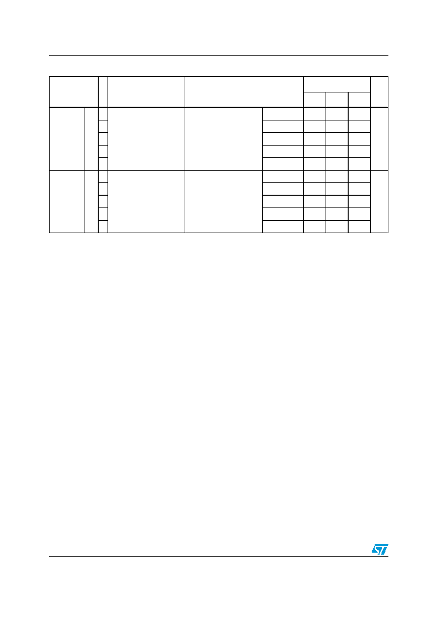
Table 25 shows the program and erase characteristics.
IDDSTDBY2 CC
P
STANDBY2 mode
current(9)
Slow internal RC
oscillator (128 kHz)
running
TA = 25 °C
—
30
100
A
DTA =55 °C
—
75
—
DTA = 85 °C
—
180
—
DTA = 105 °C
—
315
—
PTA = 125 °C
—
560
1700
IDDSTDBY1 CC
T
STANDBY1 mode
current(10)
Slow internal RC
oscillator (128 kHz)
running
TA =25 °C
—
20
60
A
DTA =55 °C
—
45
—
DTA = 85 °C
—
100
—
DTA = 105 °C
—
165
—
DTA = 125 °C
—
280
900
1.
VDD = 3.3 V ± 10% / 5.0 V ± 10%, TA = 40 to 125 °C, unless otherwise specified
2.
Running consumption is given on voltage regulator supply (VDDREG). IDDMAX is composed of three components: IDDMAX =
IDD(vdd_bv) + IDD(vdd_hv) + IDD(Vdd_hv_adc). It does not include a fourth component linked to I/Os toggling which is
highly dependent on the application. The given value is thought to be a worst case value with all peripherals running, and
code fetched from code flash while modify operation on-going on data flash. It is to be noticed that this value can be
significantly reduced by application: switch-off not used peripherals (default), reduce peripheral frequency through internal
prescaler, fetch from RAM most used functions, use low power mode when possible.
3.
Higher current may be sinked by device during power-up and standby exit. please refer to in rush current on Table 22.
4.
RUN current measured with typical application with accesses on both flash and RAM.
5.
Only for the “P” classification: Data and Code Flash in Normal Power. Code fetched from RAM: Serial IPs CAN and LIN in
loop back mode, DSPi as Master, PLL as system Clock (4 x Multiplier) peripherals on (eMIOS/CTU/ADC) and running at
max frequency, periodic SW/WDG timer reset enabled.
6.
Data Flash Power Down. Code Flash in Low Power. RC-osc128kHz & RC-OSC 16MHz on. 10MHz XTAL clock. FlexCAN:
instances: 0, 1, 2 ON (clocked but not reception or transmission), instances: 4, 5, 6 clock gated. LINFlex: instances: 0, 1, 2
ON (clocked but not reception or transmission), instance: 3 clock gated. eMIOS: instance: 0 ON (16 channels on PA[0]-
PA[11] and PC[12]-PC[15]) with PWM 20kHz, instance: 1 clock gated. DSPI: instance: 0 (clocked but no communication).
RTC/API ON.PIT ON. STM ON. ADC ON but not conversion except 2 analogue watchdog
7.
Only for the “P” classification: No clock, RC 16MHz off, RC128kHz on, PLL off, HPvreg off, ULPVreg/LPVreg on. All
possible peripherals off and clock gated. Flash in power down mode.
8.
When going from RUN to STOP mode and the core consumption is > 6 mA , it is normal operation for the main regulator
module to be kept on by the on-chip current monitoring circuit. This is most likely to occur with junction temperatures
exceeding 125 °C and under these circumstances , it is possible for the current to initially exceed the maximum STOP
specification by up to 2 mA. After entering stop, the application junction temperature will reduce to the ambient level and
the main regulator will be automatically switched off when the load current is below 6 mA.
9.
Only for the “P” classification: ULPreg on, HP/LPVreg off, 32kB RAM on, device configured for minimum consumption, all
possible modules switched-off.
10. ULPreg on, HP/LPVreg off, 8kB RAM on, device configured for minimum consumption, all possible modules switched-off.
Table 24.
Low voltage power domain electrical characteristics (continued)
Symbol
C
Parameter
Conditions(1)
Value
Unit
Min
Typ
Max
相关PDF资料 |
PDF描述 |
|---|---|
| SPC560P44L3CEFBY | 32-BIT, FLASH, 64 MHz, MICROCONTROLLER, PQFP100 |
| SPC560P50L3CEFBY | 32-BIT, FLASH, 64 MHz, MICROCONTROLLER, PQFP100 |
| SPC560P44L3CEFBX | 32-BIT, FLASH, 64 MHz, MICROCONTROLLER, PQFP100 |
| SPC560P50L5CEFBX | 32-BIT, FLASH, 64 MHz, MICROCONTROLLER, PQFP144 |
| SPC560P50L3CEFBX | 32-BIT, FLASH, 64 MHz, MICROCONTROLLER, PQFP100 |
相关代理商/技术参数 |
参数描述 |
|---|---|
| SPC560B50L5C6E0X | 功能描述:32位微控制器 - MCU 32-BIT Embedded MCU 64 MHz 512kB Body RoHS:否 制造商:Texas Instruments 核心:C28x 处理器系列:TMS320F28x 数据总线宽度:32 bit 最大时钟频率:90 MHz 程序存储器大小:64 KB 数据 RAM 大小:26 KB 片上 ADC:Yes 工作电源电压:2.97 V to 3.63 V 工作温度范围:- 40 C to + 105 C 封装 / 箱体:LQFP-80 安装风格:SMD/SMT |
| SPC560B50L5C6E0Y | 功能描述:32位微控制器 - MCU 32-BIT Embedded MCU 64 MHz 512kB Body RoHS:否 制造商:Texas Instruments 核心:C28x 处理器系列:TMS320F28x 数据总线宽度:32 bit 最大时钟频率:90 MHz 程序存储器大小:64 KB 数据 RAM 大小:26 KB 片上 ADC:Yes 工作电源电压:2.97 V to 3.63 V 工作温度范围:- 40 C to + 105 C 封装 / 箱体:LQFP-80 安装风格:SMD/SMT |
| SPC560B50SK | 功能描述:开发板和工具包 - ARM Raisonance Kit 512K Starter Rflasher 64 RoHS:否 制造商:Arduino 产品:Development Boards 工具用于评估:ATSAM3X8EA-AU 核心:ARM Cortex M3 接口类型:DAC, ICSP, JTAG, UART, USB 工作电源电压:3.3 V |
| SPC560B60L3C6E0X | 制造商:STMicroelectronics 功能描述:MID MICROCONTROLLER - Tape and Reel 制造商:STMicroelectronics 功能描述:IC MCU 32BIT 1MB FLASH 100LQFP |
| SPC560B60L5C6E0X | 制造商:STMicroelectronics 功能描述:IC MCU 32BIT 1MB FLASH 144LQFP |
发布紧急采购,3分钟左右您将得到回复。