- 您现在的位置:买卖IC网 > PDF目录4227 > SST25VF064C-80-4C-Q2AE-T (Microchip Technology)IC FLASH SER 64M DUAL I/O 8WSON PDF资料下载
参数资料
| 型号: | SST25VF064C-80-4C-Q2AE-T |
| 厂商: | Microchip Technology |
| 文件页数: | 7/37页 |
| 文件大小: | 0K |
| 描述: | IC FLASH SER 64M DUAL I/O 8WSON |
| 标准包装: | 2,000 |
| 系列: | SST25 |
| 格式 - 存储器: | 闪存 |
| 存储器类型: | FLASH |
| 存储容量: | 64M(8M x 8) |
| 速度: | 80MHz |
| 接口: | SPI 串行 |
| 电源电压: | 2.7 V ~ 3.6 V |
| 工作温度: | -40°C ~ 85°C |
| 封装/外壳: | 8-WDFN 裸露焊盘 |
| 供应商设备封装: | 8-WSON |
| 包装: | 带卷 (TR) |
第1页第2页第3页第4页第5页第6页当前第7页第8页第9页第10页第11页第12页第13页第14页第15页第16页第17页第18页第19页第20页第21页第22页第23页第24页第25页第26页第27页第28页第29页第30页第31页第32页第33页第34页第35页第36页第37页
�� �
�
�64� Mbit� SPI� Serial� Dual� I/O� Flash�
�A� Microchip� Technology� Company�
�SST25VF064C�
�Data� Sheet�
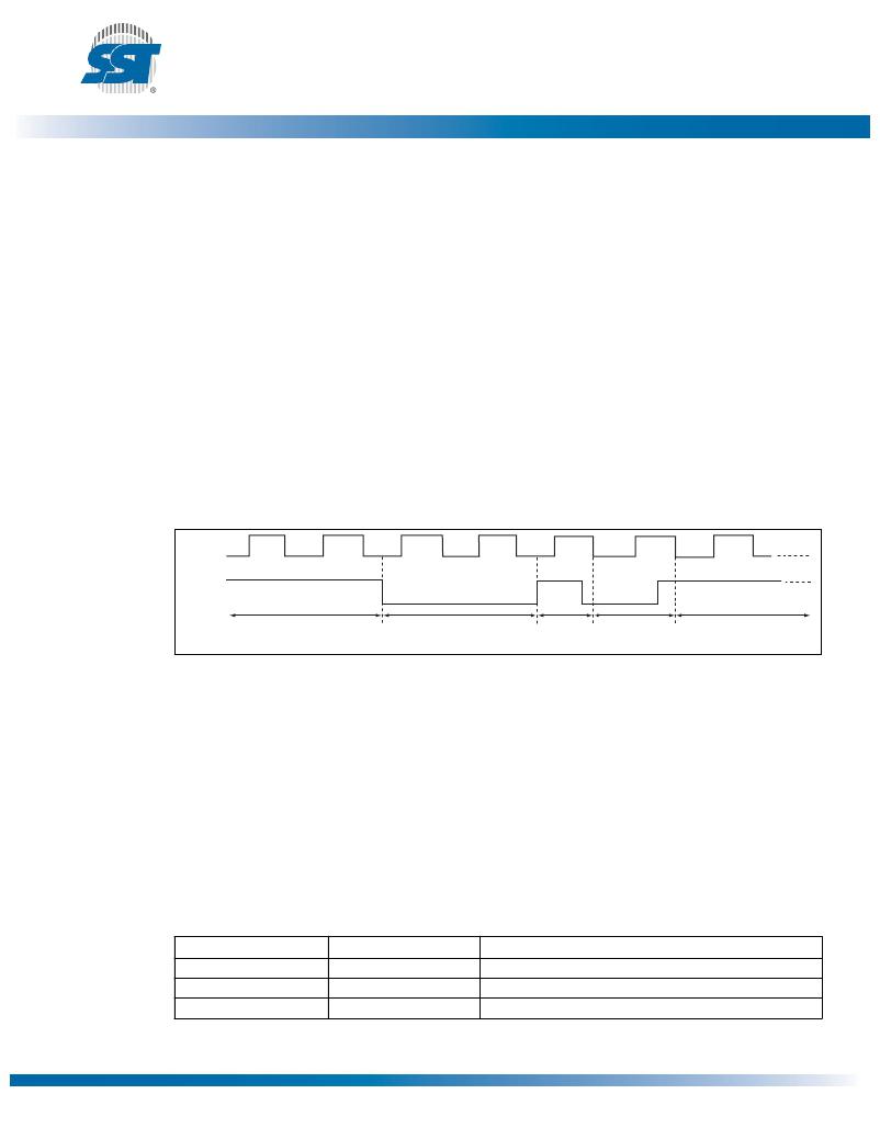
�Hold� Operation�
�The� EHLD� instruction� enables� the� hold� pin� functionality� of� the� RST#/HOLD#� pin.� Once� converted� to� a�
�hold� pin,� the� RST#/HOLD#� pin� functions� as� a� hold� pin� until� the� device� is� powered� off� and� on.� After� the�
�power� cycle,� the� pin� functionality� returns� as� a� reset� pin� (RST#)� after� the� power� on.�
�The� HOLD#� pin� is� used� to� pause� a� serial� sequence� using� the� SPI� flash� memory,� but� without� resetting�
�the� clocking� sequence.� To� activate� the� HOLD#� mode,� CE#� must� be� in� active� low� state.� The� HOLD#�
�mode� begins� when� the� SCK� active� low� state� coincides� with� the� falling� edge� of� the� HOLD#� signal.� The�
�HOLD� mode� ends� when� the� HOLD#� signal’s� rising� edge� coincides� with� the� SCK� active� low� state.�
�If� the� falling� edge� of� the� HOLD#� signal� does� not� coincide� with� the� SCK� active� low� state,� then� the� device�
�enters� Hold� mode� when� the� SCK� next� reaches� the� active� low� state.� Similarly,� if� the� rising� edge� of� the�
�HOLD#� signal� does� not� coincide� with� the� SCK� active� low� state,� then� the� device� exits� from� Hold� mode�
�when� the� SCK� next� reaches� the� active� low� state.� See� Figure� 5� for� Hold� Condition� waveform.�
�Once� the� device� enters� Hold� mode,� SO� will� be� in� high-impedance� state� while� SI� and� SCK� can� be� V� IL� or� V� IH.�
�If� CE#� is� driven� high� during� a� Hold� condition,� the� device� returns� to� Standby� mode.� As� long� as� HOLD#�
�signal� is� low,� the� memory� remains� in� the� Hold� condition.� To� resume� communication� with� the� device,�
�HOLD#� must� be� driven� active� high,� and� CE#� must� be� driven� active� low.� See� Figure� 5� for� Hold� timing.�
�SCK�
�HOLD#�
�Active�
�Hold�
�Active�
�Hold�
�Active�
�1392� F05.0�
�Figure� 5:� Hold� Condition� Waveform�
�Write� Protection�
�SST25VF064C� provides� software� Write� protection.� The� Write� Protect� pin� (WP#)� enables� or� disables�
�the� lock-down� function� of� the� status� register.� The� Block-Protection� bits� (BP3,� BP2,� BP1,� BP0,� and� BPL)�
�in� the� status� register� provide� Write� protection� to� the� memory� array� and� the� status� register.� See� Table� 5�
�for� the� Block-Protection� description.�
�Write� Protect� Pin� (WP#)�
�The� Write� Protect� (WP#)� pin� enables� the� lock-down� function� of� the� BPL� bit� (bit� 7)� in� the� status� register.�
�When� WP#� is� driven� low,� the� execution� of� the� Write-Status-Register� (WRSR)� instruction� is� determined� by�
�the� value� of� the� BPL� bit� (see� Table� 3).� When� WP#� is� high,� the� lock-down� function� of� the� BPL� bit� is� disabled.�
�Table� 3:� Conditions� to� execute� Write-Status-Register� (WRSR)� Instruction�
�WP#�
�L�
�L�
�H�
�BPL�
�1�
�0�
�X�
�Execute� WRSR� Instruction�
�Not� Allowed�
�Allowed�
�Allowed�
�T3.0� 25036�
�?2011� Silicon� Storage� Technology,� Inc.�
�7�
�DS25036A�
�06/11�
�相关PDF资料 |
PDF描述 |
|---|---|
| AMC10DTEH | CONN EDGECARD 20POS .100 EYELET |
| SST25VF064C-80-4C-Q2AE | IC FLASH SER 64M DUAL I/O 8WSON |
| ASC60DRTS | CONN EDGECARD 120PS .100 DIP SLD |
| SST25VF064C-80-4I-SCE-T | IC FLASH SER 64M DUAL I/O 16SOIC |
| XC2V1000-5FG456I | IC FPGA VIRTEX-II 456FGBGA |
相关代理商/技术参数 |
参数描述 |
|---|---|
| SST25VF064C-80-4C-Q2CE | 制造商:SST 制造商全称:Silicon Storage Technology, Inc 功能描述:64 Mbit SPI Serial Dual I/O Flash |
| SST25VF064C-80-4C-S3AE | 制造商:SST 制造商全称:Silicon Storage Technology, Inc 功能描述:64 Mbit SPI Serial Dual I/O Flash |
| SST25VF064C-80-4C-S3CE | 制造商:SST 制造商全称:Silicon Storage Technology, Inc 功能描述:64 Mbit SPI Serial Dual I/O Flash |
| SST25VF064C-80-4C-SAE | 制造商:SST 制造商全称:Silicon Storage Technology, Inc 功能描述:64 Mbit SPI Serial Dual I/O Flash |
| SST25VF064C-80-4C-SCE | 制造商:SST 制造商全称:Silicon Storage Technology, Inc 功能描述:64 Mbit SPI Serial Dual I/O Flash |
发布紧急采购,3分钟左右您将得到回复。