- 您现在的位置:买卖IC网 > PDF目录98142 > SST89E554A-40-C-NJ (SILICON STORAGE TECHNOLOGY INC) 8-BIT, FLASH, 40 MHz, MICROCONTROLLER, PQCC44 PDF资料下载
参数资料
| 型号: | SST89E554A-40-C-NJ |
| 厂商: | SILICON STORAGE TECHNOLOGY INC |
| 元件分类: | 微控制器/微处理器 |
| 英文描述: | 8-BIT, FLASH, 40 MHz, MICROCONTROLLER, PQCC44 |
| 封装: | PLASTIC, MS-018AC, LCC-44 |
| 文件页数: | 2/87页 |
| 文件大小: | 996K |
| 代理商: | SST89E554A-40-C-NJ |
第1页当前第2页第3页第4页第5页第6页第7页第8页第9页第10页第11页第12页第13页第14页第15页第16页第17页第18页第19页第20页第21页第22页第23页第24页第25页第26页第27页第28页第29页第30页第31页第32页第33页第34页第35页第36页第37页第38页第39页第40页第41页第42页第43页第44页第45页第46页第47页第48页第49页第50页第51页第52页第53页第54页第55页第56页第57页第58页第59页第60页第61页第62页第63页第64页第65页第66页第67页第68页第69页第70页第71页第72页第73页第74页第75页第76页第77页第78页第79页第80页第81页第82页第83页第84页第85页第86页第87页
10
Preliminary Specifications
FlashFlex51 MCU
SST89E554A / SST89V554A
2003 Silicon Storage Technology, Inc.
S71228-00-000
6/03
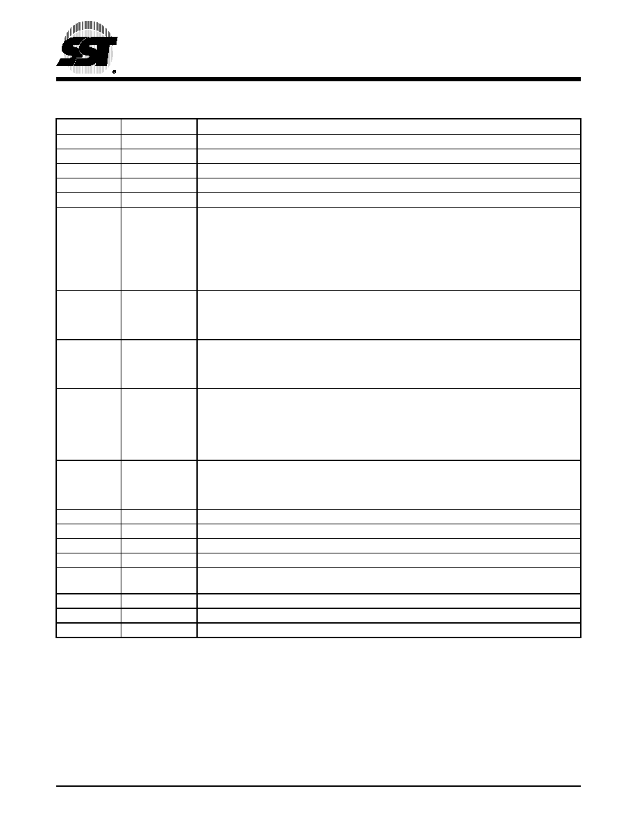
P3[3]
I
INT1#: External Interrupt 1 Input
P3[4]
I
T0: External count input to Timer/Counter 0
P3[5]
I
T1: External count input to Timer/Counter 1
P3[6]
O
WR#: External Data Memory Write strobe
P3[7]
O
RD#: External Data Memory Read strobe
PSEN#
I/O
Program Store Enable: PSEN# is the Read strobe to External Program Store. When the
device is executing from Internal Program Memory, PSEN# is inactive (VOH). When the
device is executing code from External Program Memory, PSEN# is activated twice each
machine cycle, except when access to External Data Memory while one PSEN# activation
is skipped in each machine cycle. A forced high-to-low input transition on the PSEN# pin
while the RST input is continually held high for more than ten machine cycles will cause the
device to enter External Host mode for programming.
RST
I
Reset: While the oscillator is running, a high logic state on this pin for two machine cycles
will reset the device. After a reset, if the PSEN# pin is driven by a high-to-low input transition
while the RST input pin is held high, the device will enter the External Host mode, otherwise
the device will enter the Normal operation mode.
EA#
I
External Access Enable: EA# must be driven to VIL in order to enable the device to fetch
code from the External Program Memory. EA# must be driven to VIH for internal program
execution. However, Security lock level 4 will disable EA#, and program execution is only
possible from internal program memory. The EA# pin can tolerate a high voltage2 of 12V.
ALE/PROG#
I/O
Address Latch Enable: ALE is the output signal for latching the low byte of the address
during an access to external memory. This pin is also the programming pulse input
(PROG#) for flash programming. Normally the ALE3 is emitted at a constant rate of 1/6 the
crystal frequency4 and can be used for external timing and clocking. One ALE pulse is
skipped during each access to external data memory. However, if AO is set to 1, ALE is dis-
abled.
P4[3:0]5
I/O with internal
pull-ups
Port 4: Port 4 is an 4-bit bi-directional I/O port with internal pull-ups. The port 4 output buff-
ers can drive LS TTL inputs. Port 4 pins are pulled high by the internal pull-ups when ‘1’s are
written to them and can be used as inputs in this state. As inputs, port 4 pins that are exter-
nally pulled low will source current because of the internal pull-ups.
P4[0]
I/O
Bit 0 of port 4
P4[1]
I/O
Bit 1 of port 4
P4[2] / INT3#
I/O
Bit 2 of port 4 / INT3# External interrupt 3 input
P4[3] / INT2#
I/O
Bit 3 of port 4 / INT2# External interrupt 2 input
XTAL1
I
Crystal 1: Input to the inverting oscillator amplifier and input to the internal clock generator
circuits.
XTAL2
O
Crystal 2: Output from the inverting oscillator amplifier
VDD
I
Power Supply
VSS
I
Ground
T2-1.0 1228
1. I = Input; O = Output
2. It is not necessary to receive a 12V programming supply voltage during flash programming.
3. ALE loading issue: When ALE pin experiences higher loading (>30pf) during the reset, the MCU may accidentally enter into modes
other than normal working mode. The solution is to add a pull-up resistor of 3-50 K
to VDD, e.g. for ALE pin.
4. For 6 clock mode, ALE is emitted at 1/3 of crystal frequency.
5. Port 4 is not present on the PDIP package.
TABLE
2-1: PIN DESCRIPTIONS (CONTINUED) (2 OF 2)
Symbol
Type1
Name and Functions
相关PDF资料 |
PDF描述 |
|---|---|
| SST89E554A-40-I-TQJ | 8-BIT, FLASH, 40 MHz, MICROCONTROLLER, PQFP44 |
| SSTE32882HLBAKG | SSTE SERIES, PLL BASED CLOCK DRIVER, 4 TRUE OUTPUT(S), 0 INVERTED OUTPUT(S), PBGA176 |
| SSTE32882HLBBKG | SSTE SERIES, PLL BASED CLOCK DRIVER, 4 TRUE OUTPUT(S), 0 INVERTED OUTPUT(S), PBGA176 |
| SSTUA32864EC,557 | SSTU SERIES, POSITIVE EDGE TRIGGERED D FLIP-FLOP, TRUE OUTPUT, PBGA96 |
| SSTUA32866EC/G | 32866 SERIES, POSITIVE EDGE TRIGGERED D FLIP-FLOP, COMPLEMENTARY OUTPUT, PBGA96 |
相关代理商/技术参数 |
参数描述 |
|---|---|
| SST89E554RC | 制造商:SST 制造商全称:Silicon Storage Technology, Inc 功能描述:FlashFlex51 MCU |
| SST89E554RC-25-C-NI | 制造商:SST 制造商全称:Silicon Storage Technology, Inc 功能描述:FlashFlex51 MCU |
| SST89E554RC-25-C-NJ | 制造商:SST 制造商全称:Silicon Storage Technology, Inc 功能描述:FlashFlex51 MCU |
| SST89E554RC-25-C-PI | 制造商:SST 制造商全称:Silicon Storage Technology, Inc 功能描述:FlashFlex51 MCU |
| SST89E554RC-25-C-PJ | 制造商:SST 制造商全称:Silicon Storage Technology, Inc 功能描述:FlashFlex51 MCU |
发布紧急采购,3分钟左右您将得到回复。