- 您现在的位置:买卖IC网 > PDF目录98143 > ST52T430K3B6 (STMICROELECTRONICS) 8-BIT, OTPROM, 20 MHz, MICROCONTROLLER, PDIP32 PDF资料下载
参数资料
| 型号: | ST52T430K3B6 |
| 厂商: | STMICROELECTRONICS |
| 元件分类: | 微控制器/微处理器 |
| 英文描述: | 8-BIT, OTPROM, 20 MHz, MICROCONTROLLER, PDIP32 |
| 封装: | PLASTIC, SDIP-32 |
| 文件页数: | 40/85页 |
| 文件大小: | 1192K |
| 代理商: | ST52T430K3B6 |
第1页第2页第3页第4页第5页第6页第7页第8页第9页第10页第11页第12页第13页第14页第15页第16页第17页第18页第19页第20页第21页第22页第23页第24页第25页第26页第27页第28页第29页第30页第31页第32页第33页第34页第35页第36页第37页第38页第39页当前第40页第41页第42页第43页第44页第45页第46页第47页第48页第49页第50页第51页第52页第53页第54页第55页第56页第57页第58页第59页第60页第61页第62页第63页第64页第65页第66页第67页第68页第69页第70页第71页第72页第73页第74页第75页第76页第77页第78页第79页第80页第81页第82页第83页第84页第85页
ST52T430/E430
45/85
One Channel Continuous Mode
In this mode (SEQ = ‘0’’, LP = ‘1’) a continuous
conversion flow is entered by a starting event on
the channel selected by the CH0, CH1, CH2 bits
For example: CH(2:0) = ‘011’ means continuous
conversion of channel 3. At the end of each
conversion the relative IR is updated with the last
conversion result, while the former value is lost.
To stop the conversion STR has to be set to ‘0’.
Multiple Channels Continuous Mode
In this mode (SEQ = ‘1’’, LP = ‘1’) a continuous
conversion flow is entered by a starting event on
the channels selected by the CH0, CH1, CH2 bits.
i.e CH(2:0) = ‘011’ means continuous conversion
of channel 0,1,2 and 3.
At the end of each conversion the relative IRs are
updated with the last conversion results, while the
former values are lost.
To stop the conversion STR has to be set to ‘0’.
8.2.2 Power Down Mode.
Before enabling any A/D operation mode, set the
POW bit of the A/D configuration register to ‘1’ at
least 60
s before the first conversion starts to
enable the biasing circuit inside the analog section
of the converter. Clearing the POW bit (POW = ‘0’)
is useful when the A/D is not used, reducing the
total chip power consumption. This state is also the
reset configuration and it is forced by hardware
when the core is in HALT state (after a HALT
instruction execution).
8.3 A/D Registers Description
The result of the conversions of the 8 available
channels are loaded in the 8 Input Register from
decimal address 1 to decimal address 8. (IR (1:8)
see Table 2.2)). Every IR(1:8) is reloaded with a
new value at the end of the conversion of the
correspondent analog input.
By using the assembler instruction:
LDRI RAM_Reg. IR_i
the value stored in the i-th IR is transferred on the
RAM location RAM_Reg.
The A/D configuration register is the REG_CONF
3. Figure 6.2 illustrates the structure of this
register, which manages the A/D logic operation.
The A/D configuration register (REG_CONF 3) is
programmable as following:
b7-b5 = CH2, CH1, CH0: Last Conversion
Address. These 3 bits define the last analog input.
The first analog input is converted, then the
address
is
incremented
for
the
successive
conversion until the channel identified by CH0-
CH2 is converted. The (CH2, CH1, CH0) bits
define the group of channels to be scanned. When
setting CH2=0 CH1=0 CH0=0 only channel 0 is
converted.
b4 = SCK: Master clock divider. ST52x430 can
work with a clock frequency up to 20 MHz. The
SCK must be set to ‘1’ when the ST52x430 clock is
higher then 10 MHz. It is useful to set SCK = ‘1’
even when the clock master is lower than 10 MHz
and a high accuracy is required.
b3 = SEQ: Multiple/Single channel. When SEQ is
set to ‘0’ the channel identified by CH(2:0) is
converted. If SEQ is set to ‘1’ the group of channels
identified by CH(2:0) are converted.
b2= POW: Power Up/ Power Down. A logical ‘1’
enables the A/D logic and analog circuitry.
Logical level ‘0’ disables all power consuming
logic, allowing a low power idle status.
b1 = LP: Continuous/Single. When this bit is set to
‘1’
(continuous
mode),
the
first
conversion
sequences are started by the STR bit then a
continuous conversion flow is processed.
When LP=’0’ (single mode) only one sequence of
conversions is started when STR is set.
b0 = STR: Start/Stop. A logical level ‘1’ enables
starting a conversion sequence; a logical level ‘0’
stops the conversion. When the A/D is running in
the Single Modes (LP=’0’), this bit is hardware
reset at the end of a conversion sequence.
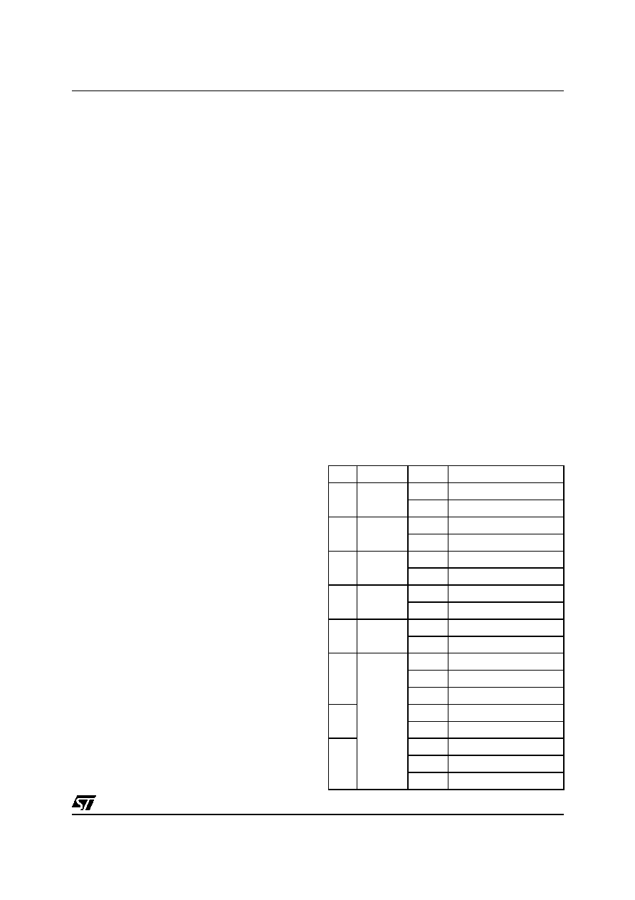
Table 8.1 A/D Conf. Register (Reg_Conf 3)
Bit
Name
Value
Description
0STR
0
Stop Conversion
1
Start Conversion
1LP
0
Single Conversion
1
Continuous
2POW
0
A/D OFF
1
A/D ON
3SEQ
0
Single Channel Conv.
1
Multiple Channels Conv
4SCK
0
Clock not Divided
1
Clock Divided
5
CH(2:0)
000
Channel 0
001
Channel 1
010
Channel 2
6
011
Channel 3
100
Channel 4
7
101
Channel 5
110
Channel 6
111
Channel 7
相关PDF资料 |
PDF描述 |
|---|---|
| ST52T430K3T6 | 8-BIT, OTPROM, 20 MHz, MICROCONTROLLER, PQFP32 |
| ST5X86V12HS | 64-BIT, 120 MHz, MICROPROCESSOR, CPGA168 |
| ST6235Q6 | 8-BIT, MROM, 8 MHz, MICROCONTROLLER, PQFP52 |
| ST6240BQ6/XXX | 8-BIT, MROM, 8 MHz, MICROCONTROLLER, PQFP80 |
| ST6242BQ1/XXX | 8-BIT, MROM, 8 MHz, MICROCONTROLLER, PQFP64 |
相关代理商/技术参数 |
参数描述 |
|---|---|
| ST52T430K3M6 | 制造商:STMicroelectronics 功能描述: |
| ST52T430K3T6 | 制造商:STMICROELECTRONICS 制造商全称:STMicroelectronics 功能描述:8-BIT INTELLIGENT CONTROLLER UNIT ICU Three Timer/PWMs, ADC, SCI |
| ST52T440 | 制造商:STMICROELECTRONICS 制造商全称:STMicroelectronics 功能描述:8-BIT INTELLIGENT CONTROLLER UNIT ICU Timer/PWM, Analog Comparator, Triac/PWM Timer, WDG |
| ST52T440F0B6 | 制造商:STMICROELECTRONICS 制造商全称:STMicroelectronics 功能描述:8-BIT INTELLIGENT CONTROLLER UNIT ICU Timer/PWM, Analog Comparator, Triac/PWM Timer, WDG |
| ST52T440F0M6 | 制造商:STMICROELECTRONICS 制造商全称:STMicroelectronics 功能描述:8-BIT INTELLIGENT CONTROLLER UNIT ICU Timer/PWM, Analog Comparator, Triac/PWM Timer, WDG |
发布紧急采购,3分钟左右您将得到回复。