- 您现在的位置:买卖IC网 > PDF目录98143 > ST52T430K3B6 (STMICROELECTRONICS) 8-BIT, OTPROM, 20 MHz, MICROCONTROLLER, PDIP32 PDF资料下载
参数资料
| 型号: | ST52T430K3B6 |
| 厂商: | STMICROELECTRONICS |
| 元件分类: | 微控制器/微处理器 |
| 英文描述: | 8-BIT, OTPROM, 20 MHz, MICROCONTROLLER, PDIP32 |
| 封装: | PLASTIC, SDIP-32 |
| 文件页数: | 61/85页 |
| 文件大小: | 1192K |
| 代理商: | ST52T430K3B6 |
第1页第2页第3页第4页第5页第6页第7页第8页第9页第10页第11页第12页第13页第14页第15页第16页第17页第18页第19页第20页第21页第22页第23页第24页第25页第26页第27页第28页第29页第30页第31页第32页第33页第34页第35页第36页第37页第38页第39页第40页第41页第42页第43页第44页第45页第46页第47页第48页第49页第50页第51页第52页第53页第54页第55页第56页第57页第58页第59页第60页当前第61页第62页第63页第64页第65页第66页第67页第68页第69页第70页第71页第72页第73页第74页第75页第76页第77页第78页第79页第80页第81页第82页第83页第84页第85页
ST52T430/E430
64/85
A frame error can occur if the parity check hasn’t
been successfully achieved or if the STOP bit
hasn’t been detected.
If
the
Recovery
Buffer
Block
receives
10
consecutive bits at logic level 0, a break error
occurs and an interrupt routine request starts.
SCDR_RX Block
It is a finite state machine synchronized with the
clock master signal, CKM.
The SCDR_RX block waits for the signal of
complete reception from the Recovery Buffer, in
order to load the word received. Moreover, the
SCDR_RX block loads the values of FRERR and
NSERR flag bits (Input Register 19), and sets the
RXF flag to 1.
Data is transferred to RAM and the RXF flag is
reset to 0 by using the LDRI instruction in order to
indicate that the SCDR_RX block is empty.
If new data arrives before the previous one has
been transferred to Register File, an overrun error
occurs and OVERR flag of Input Register 19 is set
to 1.
Warning: The SCI looses synchronization in data
reception
when
two
bytes
are
received
consecutively, without an idle time of at least 3/16
of bit time (3 SCI CLOCK_RX cycles).
To avoid lost of synchronization when two
consecutive bytes are received by the ST52x430
SCI peripheral, the external Transmitter device
must guarantee an idle time corresponding to 3
CLOCK_RX cycles between the stop bit of each
byte and the start bit of the successive byte.
As an implementation suggestion, this can be
achieved by configuring the external Transmitter
device with 2 Stop bits and the ST52x430 SCI
configured as a Receiver with 1 Stop bit.
11.2 SCI Transmitter Block
The SCI Transmitter Block consists of the following
blocks:
SCDR_TX
and
SHIFT
REGISTER,
synchronized, respectively, with the clock master
signal (CKM) and the CLOCK_TX.
The whole block receives the settings for the
following transmission modes (see Table 11.1)
through Configuration Register 20 (M bits):
I 8-bit word and a single stop signal
I 8-bit word plus a parity bit and a single stop
signal
I 8-bit word plus a double stop signal
I 9-bit word
In case of 9 bit frame transmission, the most
significative
bit
arrives
through
T8
of
the
Configuration Register 20.
Instead, in an 8-bit transmission T8 is used to
configure SCI according to information contained
in M (see Table 11.1). In particular, it is used to
choose the polarity control (even or odds) in order
to implement the parity check.
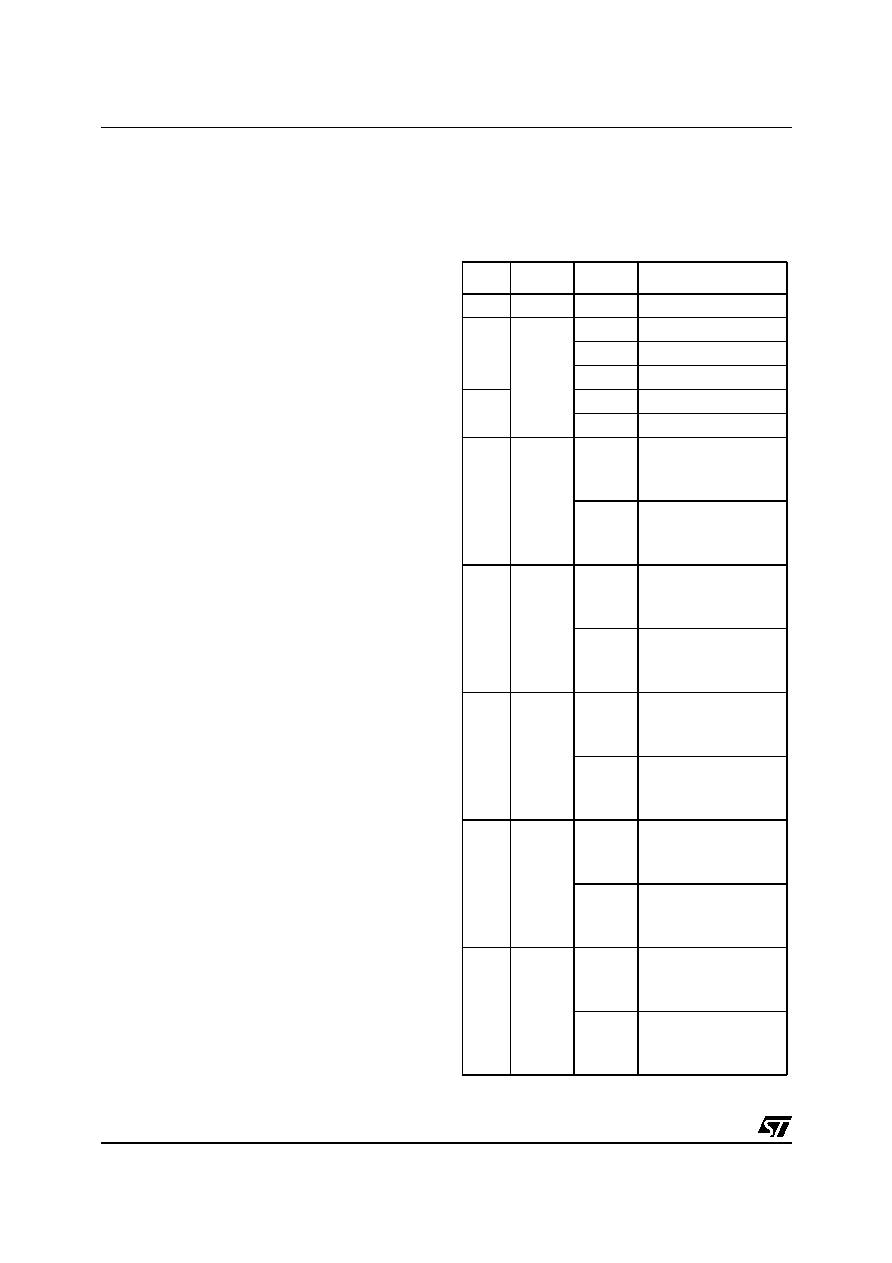
Table 11.2 Configuration Register 19 Setting
Bit
Name
Value
Description
0
-
Not used
1
ECKF
00
5 MHz
01
10 MHz
2
10
20 MHz
11
5 MHz
3TXC
0
SCI End
Transmission
Interrupt Disabled
1
SCI End
Transmission
Interrupt Enabled
4TDRE
0
SCI Transmission
Data Register Empty
Interrupt Disabled
1
SCI Transmission
Data Register Empty
Interrupt Enabled
5BRK
0
SCI Break Error
Interrupt Disabled
1
SCI Break Error
Interrupt Enabled
6OVR
0
SCI Overrun Error
Interrupt Disabled
1
SCI Overrun Error
Interrupt Enabled
7RDRF
0
SCI Received Data
Register Full Interrupt
Disabled
1
SCI Received Data
Register Full Interrupt
Enabled
相关PDF资料 |
PDF描述 |
|---|---|
| ST52T430K3T6 | 8-BIT, OTPROM, 20 MHz, MICROCONTROLLER, PQFP32 |
| ST5X86V12HS | 64-BIT, 120 MHz, MICROPROCESSOR, CPGA168 |
| ST6235Q6 | 8-BIT, MROM, 8 MHz, MICROCONTROLLER, PQFP52 |
| ST6240BQ6/XXX | 8-BIT, MROM, 8 MHz, MICROCONTROLLER, PQFP80 |
| ST6242BQ1/XXX | 8-BIT, MROM, 8 MHz, MICROCONTROLLER, PQFP64 |
相关代理商/技术参数 |
参数描述 |
|---|---|
| ST52T430K3M6 | 制造商:STMicroelectronics 功能描述: |
| ST52T430K3T6 | 制造商:STMICROELECTRONICS 制造商全称:STMicroelectronics 功能描述:8-BIT INTELLIGENT CONTROLLER UNIT ICU Three Timer/PWMs, ADC, SCI |
| ST52T440 | 制造商:STMICROELECTRONICS 制造商全称:STMicroelectronics 功能描述:8-BIT INTELLIGENT CONTROLLER UNIT ICU Timer/PWM, Analog Comparator, Triac/PWM Timer, WDG |
| ST52T440F0B6 | 制造商:STMICROELECTRONICS 制造商全称:STMicroelectronics 功能描述:8-BIT INTELLIGENT CONTROLLER UNIT ICU Timer/PWM, Analog Comparator, Triac/PWM Timer, WDG |
| ST52T440F0M6 | 制造商:STMICROELECTRONICS 制造商全称:STMicroelectronics 功能描述:8-BIT INTELLIGENT CONTROLLER UNIT ICU Timer/PWM, Analog Comparator, Triac/PWM Timer, WDG |
发布紧急采购,3分钟左右您将得到回复。