- 您现在的位置:买卖IC网 > PDF目录98145 > ST72651AR6T1E/XXX (STMICROELECTRONICS) 8-BIT, MROM, MICROCONTROLLER, PQFP64 PDF资料下载
参数资料
| 型号: | ST72651AR6T1E/XXX |
| 厂商: | STMICROELECTRONICS |
| 元件分类: | 微控制器/微处理器 |
| 英文描述: | 8-BIT, MROM, MICROCONTROLLER, PQFP64 |
| 封装: | 10 X 10 MM, ROHS COMPLIANT, TQFP-64 |
| 文件页数: | 83/161页 |
| 文件大小: | 2656K |
| 代理商: | ST72651AR6T1E/XXX |
第1页第2页第3页第4页第5页第6页第7页第8页第9页第10页第11页第12页第13页第14页第15页第16页第17页第18页第19页第20页第21页第22页第23页第24页第25页第26页第27页第28页第29页第30页第31页第32页第33页第34页第35页第36页第37页第38页第39页第40页第41页第42页第43页第44页第45页第46页第47页第48页第49页第50页第51页第52页第53页第54页第55页第56页第57页第58页第59页第60页第61页第62页第63页第64页第65页第66页第67页第68页第69页第70页第71页第72页第73页第74页第75页第76页第77页第78页第79页第80页第81页第82页当前第83页第84页第85页第86页第87页第88页第89页第90页第91页第92页第93页第94页第95页第96页第97页第98页第99页第100页第101页第102页第103页第104页第105页第106页第107页第108页第109页第110页第111页第112页第113页第114页第115页第116页第117页第118页第119页第120页第121页第122页第123页第124页第125页第126页第127页第128页第129页第130页第131页第132页第133页第134页第135页第136页第137页第138页第139页第140页第141页第142页第143页第144页第145页第146页第147页第148页第149页第150页第151页第152页第153页第154页第155页第156页第157页第158页第159页第160页第161页
ST72651AR6
28/161
Doc ID 7215 Rev 4
RESET SEQUENCE MANAGER (Cont’d)
6.2.2 Asynchronous External RESET pin
The RESET pin is both an input and an open-drain
output with integrated RON weak pull-up resistor.
This pull-up has no fixed value but varies in ac-
cordance with the input voltage. It can be pulled
low by external circuitry to reset the device. See
electrical characteristics section for more details.
A RESET signal originating from an external
source must have a duration of at least th(RSTL)in in
order to be recognized. This detection is asynchro-
nous and therefore the MCU can enter reset state
even in HALT mode.
The RESET pin is an asynchronous signal which
plays a major role in EMS performance. In a noisy
environment, it is recommended to follow the
guidelines mentioned in the electrical characteris-
tics section.
If the external RESET pulse is shorter than
signal on the RESET pin will be stretched. Other-
wise the delay will not be applied (see long ext.
Reset in Figure 17).
Starting from the external RESET pulse recogni-
tion, the device RESET pin acts as an output that
is pulled low during at least tw(RSTL)out.
6.2.3 Internal Low Voltage Detection RESET
Two different RESET sequences caused by the in-
ternal LVD circuitry can be distinguished:
■ Power-On RESET
■ Voltage Drop RESET
The device RESET pin acts as an output that is
pulled low when VDD<VIT+ (rising edge) or
The LVD filters spikes on VDD shorter than tg(VDD)
to avoid parasitic resets.
6.2.4 Internal Watchdog RESET
The RESET sequence generated by a internal
Watchdog counter overflow is shown in Figure 17.
Starting from the Watchdog counter underflow, the
device RESET pin acts as an output that is pulled
low during at least tw(RSTL)out.
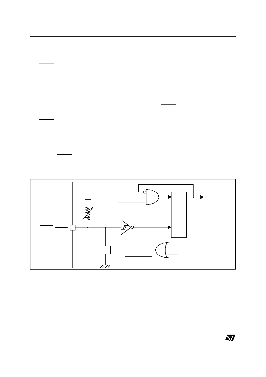
Figure 18. Reset Block Diagram
fCPU
CO
UN
TER
RESET
RON
VDD
WATCHDOG RESET
LVD RESET
INTERNAL
RESET
PULSE
GENERATOR
1
相关PDF资料 |
PDF描述 |
|---|---|
| ST72652C4T1/XXX | 8-BIT, MROM, MICROCONTROLLER, PQFP48 |
| ST7267R8T1L/XXX | 16-BIT, MROM, 30 MHz, RISC MICROCONTROLLER, PQFP64 |
| ST7267C8T1/XXX | 16-BIT, MROM, 30 MHz, RISC MICROCONTROLLER, PQFP48 |
| ST72774S9T1/XXX | 8-BIT, MROM, 8 MHz, MICROCONTROLLER, PQFP44 |
| ST72E734J6D0 | 8-BIT, UVPROM, 8 MHz, MICROCONTROLLER, CDIP42 |
相关代理商/技术参数 |
参数描述 |
|---|---|
| ST7265X-EVAL/MS | 制造商:STMicroelectronics 功能描述:ST6 EVAL BD - Bulk |
| ST7265X-EVAL/PFD | 制造商:STMicroelectronics 功能描述:USB FLASH EVAL - Bulk |
| ST7266 | 制造商:6940 功能描述:ST7266 |
| ST7267C8T1L | 制造商:STMicroelectronics 功能描述: |
| ST72681/R12 | 制造商:STMicroelectronics 功能描述:CONTROLLER FOR HIGH-PERFORMANCE BUS-POWERED USB 2.0 FLASH DR - Trays |
发布紧急采购,3分钟左右您将得到回复。