- 您现在的位置:买卖IC网 > PDF目录69367 > ST72F324K2B1 (STMICROELECTRONICS) 8-BIT, FLASH, 8 MHz, MICROCONTROLLER, PDIP32 PDF资料下载
参数资料
| 型号: | ST72F324K2B1 |
| 厂商: | STMICROELECTRONICS |
| 元件分类: | 微控制器/微处理器 |
| 英文描述: | 8-BIT, FLASH, 8 MHz, MICROCONTROLLER, PDIP32 |
| 封装: | 0.400 INCH, SHRINK, PLASTIC, DIP-32 |
| 文件页数: | 131/156页 |
| 文件大小: | 1012K |
| 代理商: | ST72F324K2B1 |
第1页第2页第3页第4页第5页第6页第7页第8页第9页第10页第11页第12页第13页第14页第15页第16页第17页第18页第19页第20页第21页第22页第23页第24页第25页第26页第27页第28页第29页第30页第31页第32页第33页第34页第35页第36页第37页第38页第39页第40页第41页第42页第43页第44页第45页第46页第47页第48页第49页第50页第51页第52页第53页第54页第55页第56页第57页第58页第59页第60页第61页第62页第63页第64页第65页第66页第67页第68页第69页第70页第71页第72页第73页第74页第75页第76页第77页第78页第79页第80页第81页第82页第83页第84页第85页第86页第87页第88页第89页第90页第91页第92页第93页第94页第95页第96页第97页第98页第99页第100页第101页第102页第103页第104页第105页第106页第107页第108页第109页第110页第111页第112页第113页第114页第115页第116页第117页第118页第119页第120页第121页第122页第123页第124页第125页第126页第127页第128页第129页第130页当前第131页第132页第133页第134页第135页第136页第137页第138页第139页第140页第141页第142页第143页第144页第145页第146页第147页第148页第149页第150页第151页第152页第153页第154页第155页第156页
ST72324J/K
76/156
10.4 SERIAL PERIPHERAL INTERFACE (SPI)
10.4.1 Introduction
The Serial Peripheral Interface (SPI) allows full-
duplex, synchronous, serial communication with
external devices. An SPI system may consist of a
master and one or more slaves or a system in
which devices may be either masters or slaves.
The SPI is normally used for communication be-
tween the microcontroller and external peripherals
or another microcontroller.
Refer to the Pin Description chapter for the device-
specific pin-out.
10.4.2 Main Features
s
Full duplex, three-wire synchronous transfers
s
Simplex, two wire synchronous transfers
s
Master or slave operation selectable either
through software or hardware
s
Six master mode frequencies (max. fCPU/4)
s
Maximum slave mode frequency = fCPU/2.
s
Programmable clock polarity and phase
s
End of transfer interrupt flag
s
Write collision flag protection
s
Master mode fault protection capability.
s
Overrun error detection flag.
10.4.3 General Description
The SPI is connected to external devices through
4(3) alternate pins:
– MISO: Master In / Slave Out pin
– MOSI: Master Out / Slave In pin
– SCK: Serial Clock pin
– SS: Slave select pin (if not done through soft-
ware)
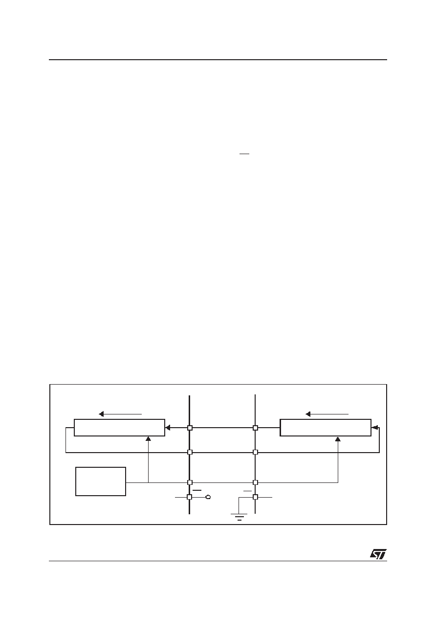
A basic example of interconnections between a
single master and a single slave is illustrated on
Figure 52.
The MOSI pins are connected together as are
MISO pins. In this way data is transferred serially
between master and slave (most significant bit
first).
When the master device transmits data to a slave
device via MOSI pin, the slave device responds by
sending data to the master device via the MISO
pin. This implies full duplex transmission with both
data out and data in synchronized with the same
clock signal (which is provided by the master de-
vice via the SCK pin).
Thus, the byte transmitted is replaced by the byte
received and eliminates the need for separate
transmit-empty and receiver-full bits. A status flag
is used to indicate that the I/O operation is com-
plete.
Four possible data/clock timing relationships may
be chosen (see Figure 55) but master and slave
must be programmed with the same timing mode.
Figure 47. Serial Peripheral Interface Master/Slave
8-BIT SHIFT REGISTER
SPI
CLOCK
GENERATOR
8-BIT SHIFT REGISTER
MISO
MOSI
MISO
SCK
SLAVE
MASTER
SS
+5V
MSBit
LSBit
MSBit
LSBit
相关PDF资料 |
PDF描述 |
|---|---|
| ST72F324K6B1 | 8-BIT, FLASH, 8 MHz, MICROCONTROLLER, PDIP32 |
| ST72F324J4B1 | 8-BIT, FLASH, 8 MHz, MICROCONTROLLER, PDIP42 |
| ST72F324J6B3 | 8-BIT, FLASH, 8 MHz, MICROCONTROLLER, PDIP42 |
| ST72F324K2B3 | 8-BIT, FLASH, 8 MHz, MICROCONTROLLER, PDIP32 |
| ST72F324K4B5 | 8-BIT, FLASH, 8 MHz, MICROCONTROLLER, PDIP32 |
相关代理商/技术参数 |
参数描述 |
|---|---|
| ST72F324K2B6 | 功能描述:8位微控制器 -MCU 5V RANGE 8B MCU RoHS:否 制造商:Silicon Labs 核心:8051 处理器系列:C8051F39x 数据总线宽度:8 bit 最大时钟频率:50 MHz 程序存储器大小:16 KB 数据 RAM 大小:1 KB 片上 ADC:Yes 工作电源电压:1.8 V to 3.6 V 工作温度范围:- 40 C to + 105 C 封装 / 箱体:QFN-20 安装风格:SMD/SMT |
| ST72F324K2T3 | 制造商:STMicroelectronics 功能描述: |
| ST72F324K2T3TR | 制造商:STMicroelectronics 功能描述: |
| ST72F324K2T6 | 功能描述:8位微控制器 -MCU Flash 8K SPI/SCI RoHS:否 制造商:Silicon Labs 核心:8051 处理器系列:C8051F39x 数据总线宽度:8 bit 最大时钟频率:50 MHz 程序存储器大小:16 KB 数据 RAM 大小:1 KB 片上 ADC:Yes 工作电源电压:1.8 V to 3.6 V 工作温度范围:- 40 C to + 105 C 封装 / 箱体:QFN-20 安装风格:SMD/SMT |
| ST72F324K2T6TR | 功能描述:8位微控制器 -MCU 8 BITS MICROCONTR RoHS:否 制造商:Silicon Labs 核心:8051 处理器系列:C8051F39x 数据总线宽度:8 bit 最大时钟频率:50 MHz 程序存储器大小:16 KB 数据 RAM 大小:1 KB 片上 ADC:Yes 工作电源电压:1.8 V to 3.6 V 工作温度范围:- 40 C to + 105 C 封装 / 箱体:QFN-20 安装风格:SMD/SMT |
发布紧急采购,3分钟左右您将得到回复。