- 您现在的位置:买卖IC网 > PDF目录69367 > ST72F324K2B1 (STMICROELECTRONICS) 8-BIT, FLASH, 8 MHz, MICROCONTROLLER, PDIP32 PDF资料下载
参数资料
| 型号: | ST72F324K2B1 |
| 厂商: | STMICROELECTRONICS |
| 元件分类: | 微控制器/微处理器 |
| 英文描述: | 8-BIT, FLASH, 8 MHz, MICROCONTROLLER, PDIP32 |
| 封装: | 0.400 INCH, SHRINK, PLASTIC, DIP-32 |
| 文件页数: | 56/156页 |
| 文件大小: | 1012K |
| 代理商: | ST72F324K2B1 |
第1页第2页第3页第4页第5页第6页第7页第8页第9页第10页第11页第12页第13页第14页第15页第16页第17页第18页第19页第20页第21页第22页第23页第24页第25页第26页第27页第28页第29页第30页第31页第32页第33页第34页第35页第36页第37页第38页第39页第40页第41页第42页第43页第44页第45页第46页第47页第48页第49页第50页第51页第52页第53页第54页第55页当前第56页第57页第58页第59页第60页第61页第62页第63页第64页第65页第66页第67页第68页第69页第70页第71页第72页第73页第74页第75页第76页第77页第78页第79页第80页第81页第82页第83页第84页第85页第86页第87页第88页第89页第90页第91页第92页第93页第94页第95页第96页第97页第98页第99页第100页第101页第102页第103页第104页第105页第106页第107页第108页第109页第110页第111页第112页第113页第114页第115页第116页第117页第118页第119页第120页第121页第122页第123页第124页第125页第126页第127页第128页第129页第130页第131页第132页第133页第134页第135页第136页第137页第138页第139页第140页第141页第142页第143页第144页第145页第146页第147页第148页第149页第150页第151页第152页第153页第154页第155页第156页
ST72324J/K
149/156
ST72324J/K DEVICE CONFIGURATION AND ORDERING INFORMATION (Cont’d)
OPT8 = PLL OFF
PLL activation
This option bit activates the PLL which allows mul-
tiplication by two of the main input clock frequency.
The PLL is guaranteed only with an input frequen-
cy between 2 and 4MHz.
0: PLL x2 enabled
1: PLL x2 disabled
CAUTION: the PLL can be enabled only if the
“OSC RANGE” (OPT11:9) bits are configured to
“MP - 2~4MHz”. Otherwise, the device functionali-
ty is not guaranteed.
OPT7= WDG HALT
Watchdog and HALT mode
This option bit determines if a RESET is generated
when entering HALT mode while the Watchdog is
active.
0: No Reset generation when entering Halt mode
1: Reset generation when entering Halt mode
OPT6= WDG SW
Hardware or software watchdog
This option bit selects the watchdog type.
0: Hardware (watchdog always enabled)
1: Software (watchdog to be enabled by software)
OPT5 = CSS
Clock security system on/off
This option bit enables or disables the clock secu-
rity system function (CSS) which include the clock
filter and the backup safe oscillator.
0: CSS enabled
1: CSS disabled
When enabled, the selected “OSC RANGE” is
used to determine which is the selected operating
frequency range to switch to the backup oscillator
when the frequency is out of range.
OPT4:3= VD[1:0]
Voltage detection
These option bits enable the voltage detection
block (LVD, and AVD) with a selected threshold for
the LVD and AVD (EVD+IVD).
OPT0= FMP_R
Flash memory read-out protection
This option indicates if the user flash memory is
protected against read-out piracy. This protection
is based on read and a write protection of the
memory in test modes and ICP mode. Erasing the
option bytes when the FMP_R option is selected
induce the whole user memory erasing first.
0: read-out protection enabled
1: read-out protection disabled
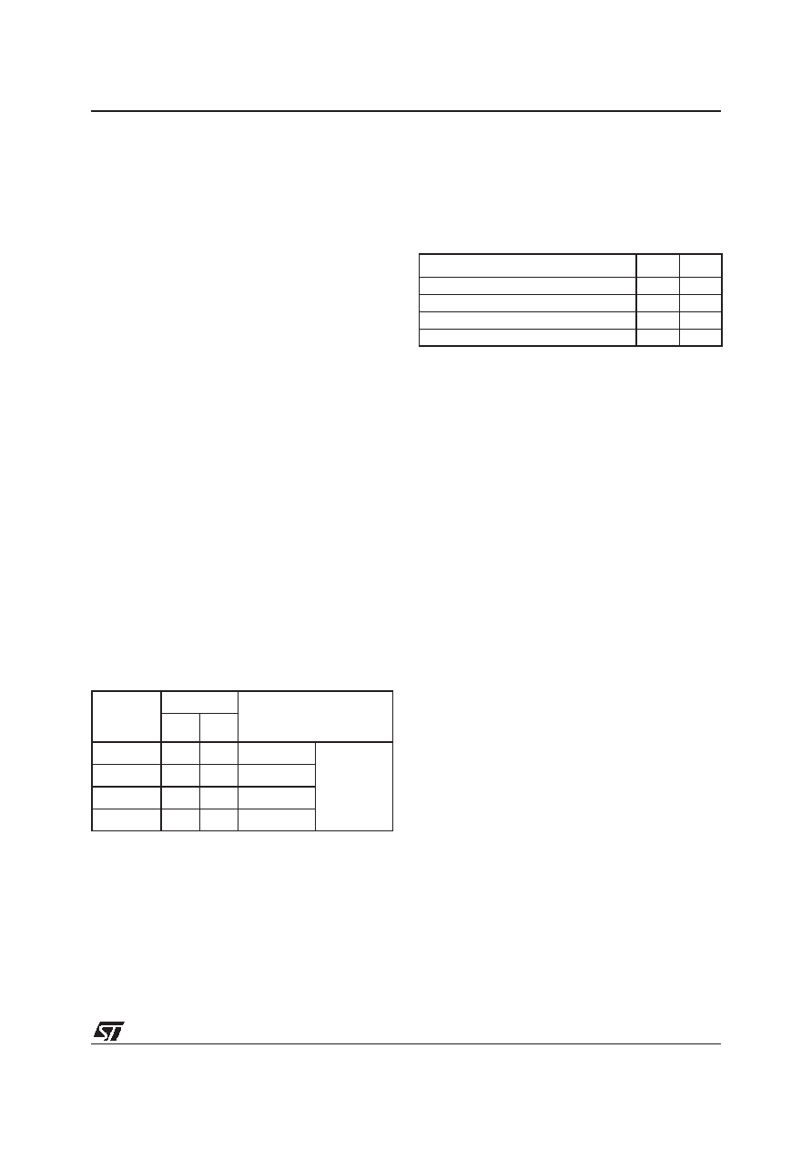
Typ. Freq.
Range
OSCRANGE Compared frequencies to
decide to switch to the
backup oscillator
10
1~2MHz
0
2 x fCPU
fSFOSC
2~4MHz
0
1
fCPU
4~8MHz
1
0
fCPU/2
8~16MHz
1
fCPU/4
Selected Low Voltage Detector
VD1
VD0
LVD and AVD Off
1
Lowest Voltage Threshold (VDD~3.5V)
1
0
Medium Voltage Threshold (VDD~4V)
0
1
Highest Voltage Threshold (VDD~5V)
0
相关PDF资料 |
PDF描述 |
|---|---|
| ST72F324K6B1 | 8-BIT, FLASH, 8 MHz, MICROCONTROLLER, PDIP32 |
| ST72F324J4B1 | 8-BIT, FLASH, 8 MHz, MICROCONTROLLER, PDIP42 |
| ST72F324J6B3 | 8-BIT, FLASH, 8 MHz, MICROCONTROLLER, PDIP42 |
| ST72F324K2B3 | 8-BIT, FLASH, 8 MHz, MICROCONTROLLER, PDIP32 |
| ST72F324K4B5 | 8-BIT, FLASH, 8 MHz, MICROCONTROLLER, PDIP32 |
相关代理商/技术参数 |
参数描述 |
|---|---|
| ST72F324K2B6 | 功能描述:8位微控制器 -MCU 5V RANGE 8B MCU RoHS:否 制造商:Silicon Labs 核心:8051 处理器系列:C8051F39x 数据总线宽度:8 bit 最大时钟频率:50 MHz 程序存储器大小:16 KB 数据 RAM 大小:1 KB 片上 ADC:Yes 工作电源电压:1.8 V to 3.6 V 工作温度范围:- 40 C to + 105 C 封装 / 箱体:QFN-20 安装风格:SMD/SMT |
| ST72F324K2T3 | 制造商:STMicroelectronics 功能描述: |
| ST72F324K2T3TR | 制造商:STMicroelectronics 功能描述: |
| ST72F324K2T6 | 功能描述:8位微控制器 -MCU Flash 8K SPI/SCI RoHS:否 制造商:Silicon Labs 核心:8051 处理器系列:C8051F39x 数据总线宽度:8 bit 最大时钟频率:50 MHz 程序存储器大小:16 KB 数据 RAM 大小:1 KB 片上 ADC:Yes 工作电源电压:1.8 V to 3.6 V 工作温度范围:- 40 C to + 105 C 封装 / 箱体:QFN-20 安装风格:SMD/SMT |
| ST72F324K2T6TR | 功能描述:8位微控制器 -MCU 8 BITS MICROCONTR RoHS:否 制造商:Silicon Labs 核心:8051 处理器系列:C8051F39x 数据总线宽度:8 bit 最大时钟频率:50 MHz 程序存储器大小:16 KB 数据 RAM 大小:1 KB 片上 ADC:Yes 工作电源电压:1.8 V to 3.6 V 工作温度范围:- 40 C to + 105 C 封装 / 箱体:QFN-20 安装风格:SMD/SMT |
发布紧急采购,3分钟左右您将得到回复。