- 您现在的位置:买卖IC网 > PDF目录69368 > ST72F521R6T5 (STMICROELECTRONICS) 8-BIT, FLASH, 8 MHz, MICROCONTROLLER, PQFP64 PDF资料下载
参数资料
| 型号: | ST72F521R6T5 |
| 厂商: | STMICROELECTRONICS |
| 元件分类: | 微控制器/微处理器 |
| 英文描述: | 8-BIT, FLASH, 8 MHz, MICROCONTROLLER, PQFP64 |
| 封装: | 14 X 14 MM, PLASTIC, TQFP-64 |
| 文件页数: | 64/198页 |
| 文件大小: | 1267K |
| 代理商: | ST72F521R6T5 |
第1页第2页第3页第4页第5页第6页第7页第8页第9页第10页第11页第12页第13页第14页第15页第16页第17页第18页第19页第20页第21页第22页第23页第24页第25页第26页第27页第28页第29页第30页第31页第32页第33页第34页第35页第36页第37页第38页第39页第40页第41页第42页第43页第44页第45页第46页第47页第48页第49页第50页第51页第52页第53页第54页第55页第56页第57页第58页第59页第60页第61页第62页第63页当前第64页第65页第66页第67页第68页第69页第70页第71页第72页第73页第74页第75页第76页第77页第78页第79页第80页第81页第82页第83页第84页第85页第86页第87页第88页第89页第90页第91页第92页第93页第94页第95页第96页第97页第98页第99页第100页第101页第102页第103页第104页第105页第106页第107页第108页第109页第110页第111页第112页第113页第114页第115页第116页第117页第118页第119页第120页第121页第122页第123页第124页第125页第126页第127页第128页第129页第130页第131页第132页第133页第134页第135页第136页第137页第138页第139页第140页第141页第142页第143页第144页第145页第146页第147页第148页第149页第150页第151页第152页第153页第154页第155页第156页第157页第158页第159页第160页第161页第162页第163页第164页第165页第166页第167页第168页第169页第170页第171页第172页第173页第174页第175页第176页第177页第178页第179页第180页第181页第182页第183页第184页第185页第186页第187页第188页第189页第190页第191页第192页第193页第194页第195页第196页第197页第198页
ST72521M/R/AR
156/198
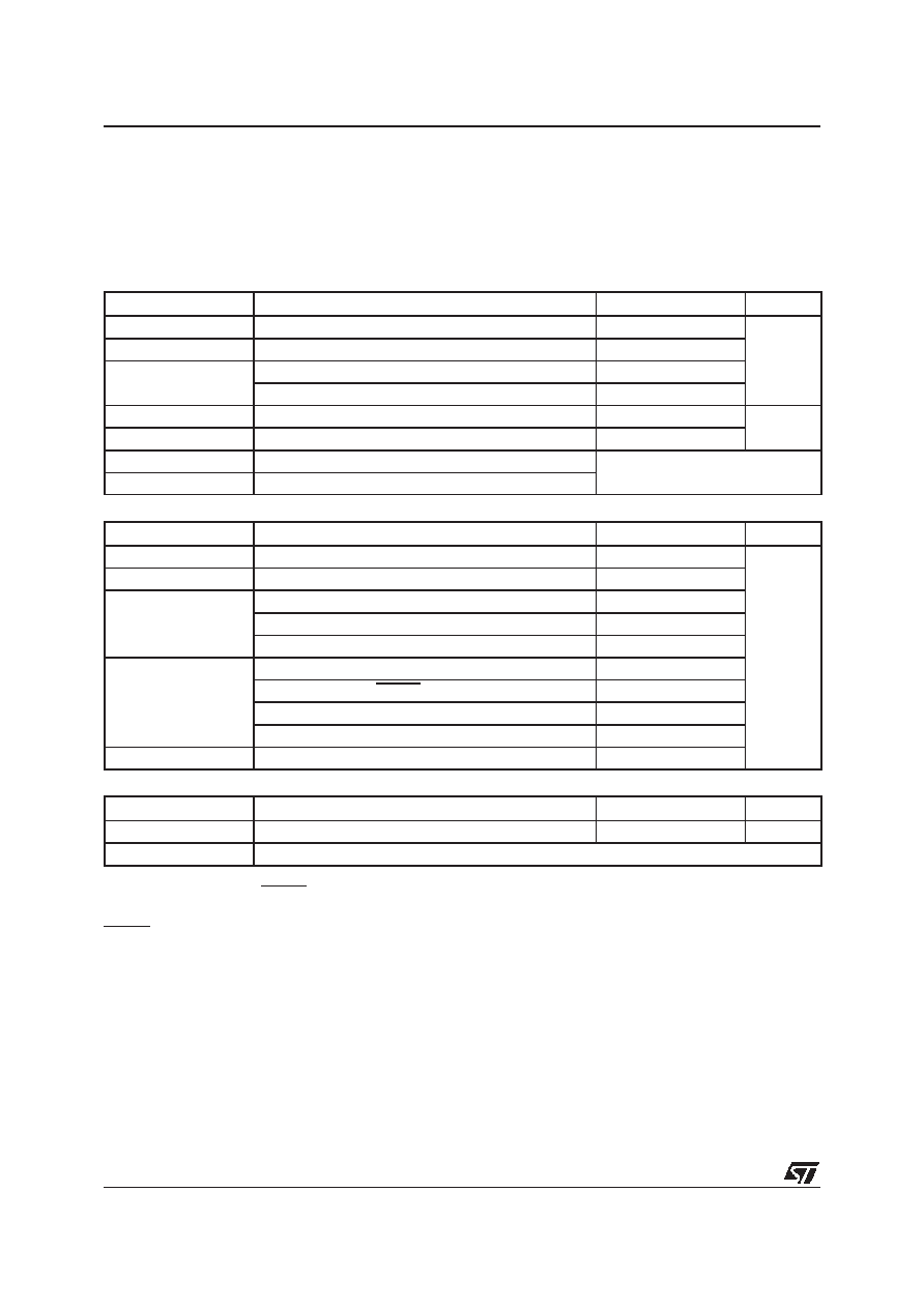
12.2 ABSOLUTE MAXIMUM RATINGS
Stresses above those listed as “absolute maxi-
mum ratings” may cause permanent damage to
the device. This is a stress rating only and func-
tional operation of the device under these condi-
tions is not implied. Exposure to maximum rating
conditions for extended periods may affect device
reliability.
12.2.1 Voltage Characteristics
12.2.2 Current Characteristics
12.2.3 Thermal Characteristics
Notes:
1. Directly connecting the RESET and I/O pins to VDD or VSS could damage the device if an unintentional internal reset
is generated or an unexpected change of the I/O configuration occurs (for example, due to a corrupted program counter).
To guarantee safe operation, this connection has to be done through a pull-up or pull-down resistor (typical: 4.7k
for
RESET, 10k
for I/Os). For the same reason, unused I/O pins must not be directly tied to V
DD or VSS.
2. When the current limitation is not possible, the VIN absolute maximum rating must be respected, otherwise refer to
IINJ(PIN) specification. A positive injection is induced by VIN>VDD while a negative injection is induced by VIN<VSS.
3. All power (VDD) and ground (VSS) lines must always be connected to the external supply.
4. Negative injection disturbs the analog performance of the device. In particular, it induces leakage currents throughout
the device including the analog inputs. To avoid undesirable effects on the analog functions, care must be taken:
- Analog input pins must have a negative injection less than 0.8 mA (assuming that the impedance of the analog voltage
is lower than the specified limits)
- Pure digital pins must have a negative injection less than 1.6mA. In addition, it is recommended to inject the current as
far as possible from the analog input pins.
5. When several inputs are submitted to a current injection, the maximum
ΣI
INJ(PIN) is the absolute sum of the positive
and negative injected currents (instantaneous values). These results are based on characterisation with
ΣI
INJ(PIN) maxi-
mum current injection on four I/O port pins of the device.
6. True open drain I/O port pins do not accept positive injection.
Symbol
Ratings
Maximum value
Unit
VDD -VSS
Supply voltage
6.5
V
VPP -VSS
Programming Voltage
14
VIN
1) & 2)
Input Voltage on true open drain pin
VSS-0.3 to 6.5
Input voltage on any other pin
VSS-0.3 to VDD+0.3
|
V
DDx| and |VSSx|
Variations between different digital power pins
50
mV
|VSSA -VSSx|
Variations between digital and analog ground pins
50
VESD(HBM)
Electro-static discharge voltage (Human Body Model)
see Section 12.7.3 on page 170
VESD(MM)
Electro-static discharge voltage (Machine Model)
Symbol
Ratings
Maximum value
Unit
IVDD
Total current into VDD power lines (source)
3)
150
mA
IVSS
Total current out of VSS ground lines (sink)
3)
150
IIO
Output current sunk by any standard I/O and control pin
25
Output current sunk by any high sink I/O pin
50
Output current source by any I/Os and control pin
- 25
IINJ(PIN)
2) & 4)
Injected current on VPP pin
± 5
Injected current on RESET pin
± 5
Injected current on OSC1 and OSC2 pins
± 5
Injected current on any other pin 5) & 6)
± 5
ΣI
INJ(PIN)
2)
Total injected current (sum of all I/O and control pins) 5)
± 25
Symbol
Ratings
Value
Unit
TSTG
Storage temperature range
-65 to +150
°C
TJ
Maximum junction temperature (see Section 13.2 THERMAL CHARACTERISTICS)
相关PDF资料 |
PDF描述 |
|---|---|
| ST72F521R7T7 | 8-BIT, FLASH, 8 MHz, MICROCONTROLLER, PQFP64 |
| ST72F521AR9TC | 8-BIT, FLASH, 8 MHz, MICROCONTROLLER, PQFP64 |
| ST72F521AR9T6 | 8-BIT, FLASH, 8 MHz, MICROCONTROLLER, PQFP64 |
| ST72521BAR6T5 | 8-BIT, MROM, 8 MHz, MICROCONTROLLER, PQFP64 |
| ST72521BR9TB | 8-BIT, MROM, 8 MHz, MICROCONTROLLER, PQFP64 |
相关代理商/技术参数 |
参数描述 |
|---|---|
| ST72F521R6T6 | 功能描述:8位微控制器 -MCU Flask 32K SPI/SCI/I2 RoHS:否 制造商:Silicon Labs 核心:8051 处理器系列:C8051F39x 数据总线宽度:8 bit 最大时钟频率:50 MHz 程序存储器大小:16 KB 数据 RAM 大小:1 KB 片上 ADC:Yes 工作电源电压:1.8 V to 3.6 V 工作温度范围:- 40 C to + 105 C 封装 / 箱体:QFN-20 安装风格:SMD/SMT |
| ST72F521R6TA | 功能描述:8位微控制器 -MCU Flask 32K SPI/SCI/I2 RoHS:否 制造商:Silicon Labs 核心:8051 处理器系列:C8051F39x 数据总线宽度:8 bit 最大时钟频率:50 MHz 程序存储器大小:16 KB 数据 RAM 大小:1 KB 片上 ADC:Yes 工作电源电压:1.8 V to 3.6 V 工作温度范围:- 40 C to + 105 C 封装 / 箱体:QFN-20 安装风格:SMD/SMT |
| ST72F521R6TATR | 功能描述:8位微控制器 -MCU AUTO 8BIT MICRO RoHS:否 制造商:Silicon Labs 核心:8051 处理器系列:C8051F39x 数据总线宽度:8 bit 最大时钟频率:50 MHz 程序存储器大小:16 KB 数据 RAM 大小:1 KB 片上 ADC:Yes 工作电源电压:1.8 V to 3.6 V 工作温度范围:- 40 C to + 105 C 封装 / 箱体:QFN-20 安装风格:SMD/SMT |
| ST72F521R6TC | 功能描述:8位微控制器 -MCU Flask 32K SPI/SCI/I2 RoHS:否 制造商:Silicon Labs 核心:8051 处理器系列:C8051F39x 数据总线宽度:8 bit 最大时钟频率:50 MHz 程序存储器大小:16 KB 数据 RAM 大小:1 KB 片上 ADC:Yes 工作电源电压:1.8 V to 3.6 V 工作温度范围:- 40 C to + 105 C 封装 / 箱体:QFN-20 安装风格:SMD/SMT |
| ST72F521R6TCTR | 功能描述:8位微控制器 -MCU AUTO 8BIT MICRO RoHS:否 制造商:Silicon Labs 核心:8051 处理器系列:C8051F39x 数据总线宽度:8 bit 最大时钟频率:50 MHz 程序存储器大小:16 KB 数据 RAM 大小:1 KB 片上 ADC:Yes 工作电源电压:1.8 V to 3.6 V 工作温度范围:- 40 C to + 105 C 封装 / 箱体:QFN-20 安装风格:SMD/SMT |
发布紧急采购,3分钟左右您将得到回复。