- 您现在的位置:买卖IC网 > PDF目录25648 > STM32W108HBU7 (STMICROELECTRONICS) SPECIALTY MICROPROCESSOR CIRCUIT, QCC40 PDF资料下载
参数资料
| 型号: | STM32W108HBU7 |
| 厂商: | STMICROELECTRONICS |
| 元件分类: | 微控制器/微处理器 |
| 英文描述: | SPECIALTY MICROPROCESSOR CIRCUIT, QCC40 |
| 封装: | 6 X 6 MM, 0.50 MM PITCH, ROHS COMPLIANT, VFQFPN-40 |
| 文件页数: | 61/198页 |
| 文件大小: | 2871K |
| 代理商: | STM32W108HBU7 |
第1页第2页第3页第4页第5页第6页第7页第8页第9页第10页第11页第12页第13页第14页第15页第16页第17页第18页第19页第20页第21页第22页第23页第24页第25页第26页第27页第28页第29页第30页第31页第32页第33页第34页第35页第36页第37页第38页第39页第40页第41页第42页第43页第44页第45页第46页第47页第48页第49页第50页第51页第52页第53页第54页第55页第56页第57页第58页第59页第60页当前第61页第62页第63页第64页第65页第66页第67页第68页第69页第70页第71页第72页第73页第74页第75页第76页第77页第78页第79页第80页第81页第82页第83页第84页第85页第86页第87页第88页第89页第90页第91页第92页第93页第94页第95页第96页第97页第98页第99页第100页第101页第102页第103页第104页第105页第106页第107页第108页第109页第110页第111页第112页第113页第114页第115页第116页第117页第118页第119页第120页第121页第122页第123页第124页第125页第126页第127页第128页第129页第130页第131页第132页第133页第134页第135页第136页第137页第138页第139页第140页第141页第142页第143页第144页第145页第146页第147页第148页第149页第150页第151页第152页第153页第154页第155页第156页第157页第158页第159页第160页第161页第162页第163页第164页第165页第166页第167页第168页第169页第170页第171页第172页第173页第174页第175页第176页第177页第178页第179页第180页第181页第182页第183页第184页第185页第186页第187页第188页第189页第190页第191页第192页第193页第194页第195页第196页第197页第198页
STM32W108CB, STM32W108HB
Analog-to-digital converter
Doc ID 16252 Rev 3
153/198
Input range
ADC inputs can be routed through input buffers to expand the input voltage range. The input
buffers have a fixed 0.25 gain and the converted data is scaled by that factor.
With the input buffers disabled the single-ended input range is 0 to VREF and the differential
input range is -VREF to +VREF. With the input buffers enabled the single-ended range is 0
to VDD_PADS and the differential range is -VDD_PADS to +VDD_PADS.
The input buffers are enabled for the ADC P and N inputs by setting the ADC_HVSELP and
ADC_HVSELN bits respectively, in the ADC_CFG register. The ADC accuracy is reduced
when the input buffer is selected.
Sample time
ADC sample time is programmed by selecting the sampling clock and the clocks per
sample.
●
The sampling clock may be either 1 MHz or 6 MHz. If the ADC_1MHZCLK bit in the
ADC_CFG register is clear, the 6 MHz clock is used; if it is set, the 1 MHz clock is
selected. The 6 MHz sample clock offers faster conversion times but the ADC
resolution is lower than that achieved with the 1 MHz clock.
●
The number of clocks per sample is determined by the ADC_PERIOD bits in the
ADC_CFG register. ADC_PERIOD values select from 32 to 4096 sampling clocks in
powers of two. Longer sample times produce more significant bits. Regardless of the
sample time, converted samples are always 16-bits in size with the significant bits left-
aligned within the value.
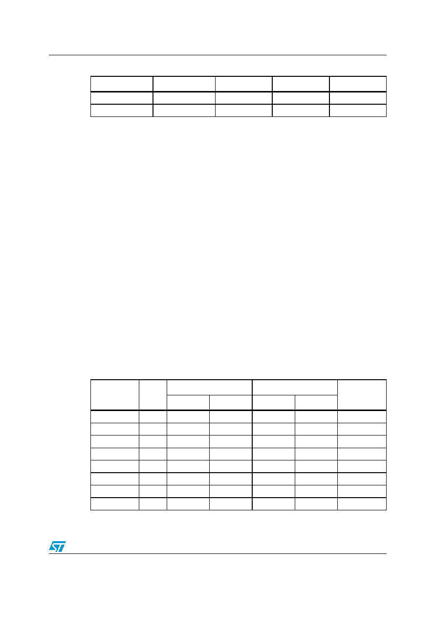
Table 30 shows the options for ADC sample times and the significant bits in the conversion
results.
VREF
VREF/2
10
9
Calibration
VDD_PADSA/2
VREF/2
11
9
Calibration
Table 30.
ADC sample times
ADC_PERIOD
Sample
Clocks
Sample Time (s)
Sample Frequency (kHz)
Significant
Bits
1 MHz clock 6 MHz clock 1 MHz clock 6 MHz clock
032
325.33
31.3
188
5
1
64
10.7
15.6
93.8
6
2
128
21.3
7.81
46.9
7
3
256
42.7
3.91
23.4
8
4
512
85.3
1.95
11.7
9
5
1024
170
0.977
5.86
10
6
2048
341
0.488
2.93
11
7
4096
682
0.244
1.47
12
Table 29.
Typical ADC input configurations (continued)
ADC P input
ADC N input
ADC_MUXP
ADC_MUXN
Purpose
相关PDF资料 |
PDF描述 |
|---|---|
| STP506C-2IW-012V | SINGLE COLOR DISPLAY CLUSTER, WHITE, 152.4 mm |
| SUGR47M | DUAL COLOR LED, RED/GREEN, 5 mm |
| SUR76D | SINGLE COLOR LED, RED, 3 mm |
| SUY17D | SINGLE COLOR LED, YELLOW, 3.9 mm |
| SY405T | SINGLE COLOR LED, AMBER, 2.7 mm |
相关代理商/技术参数 |
参数描述 |
|---|---|
| STM32WC-RFCKIT | 功能描述:Zigbee/802.15.4开发工具 STM32W Low-Cost RF STM32F103 MCU Kit RoHS:否 制造商:Silicon Labs 产品:Development Kits 工具用于评估:EM35x 频率:2.4 GHz 接口类型:USB 工作电源电压: |
| STM32W-RFCKIT | 功能描述:开发板和工具包 - 无线 STM32W RF CNTRL KIT STM32F103 USB JTAG RoHS:否 制造商:Arduino 产品:Evaluation Boards 工具用于评估:AT32UC3L 核心:AVR32 频率: 接口类型:USB 工作电源电压:5 V |
| STM3-3 | 制造商:RINO MECH.(GENGARELL 功能描述: |
| STM330 | 制造商:EnOcean GmbH 功能描述:Temperature energy harvester, 868MHz |
| STM330U | 制造商:EnOcean GmbH 功能描述:Temperature energy harvester, 315MHz 制造商:EnOcean GmbH 功能描述:Temperature energy harvester, 902MHz |
发布紧急采购,3分钟左右您将得到回复。