- 您现在的位置:买卖IC网 > PDF目录361344 > T431616E-7SG (TM Technology, Inc.) 1M x 16 SDRAM 512K x 16bit x 2Banks Synchronous DRAM PDF资料下载
参数资料
| 型号: | T431616E-7SG |
| 厂商: | TM Technology, Inc. |
| 英文描述: | 1M x 16 SDRAM 512K x 16bit x 2Banks Synchronous DRAM |
| 中文描述: | 100万× 16内存为512k × 16Bit的X 2Banks同步DRAM |
| 文件页数: | 19/74页 |
| 文件大小: | 781K |
| 代理商: | T431616E-7SG |
第1页第2页第3页第4页第5页第6页第7页第8页第9页第10页第11页第12页第13页第14页第15页第16页第17页第18页当前第19页第20页第21页第22页第23页第24页第25页第26页第27页第28页第29页第30页第31页第32页第33页第34页第35页第36页第37页第38页第39页第40页第41页第42页第43页第44页第45页第46页第47页第48页第49页第50页第51页第52页第53页第54页第55页第56页第57页第58页第59页第60页第61页第62页第63页第64页第65页第66页第67页第68页第69页第70页第71页第72页第73页第74页
TE
CH
tm
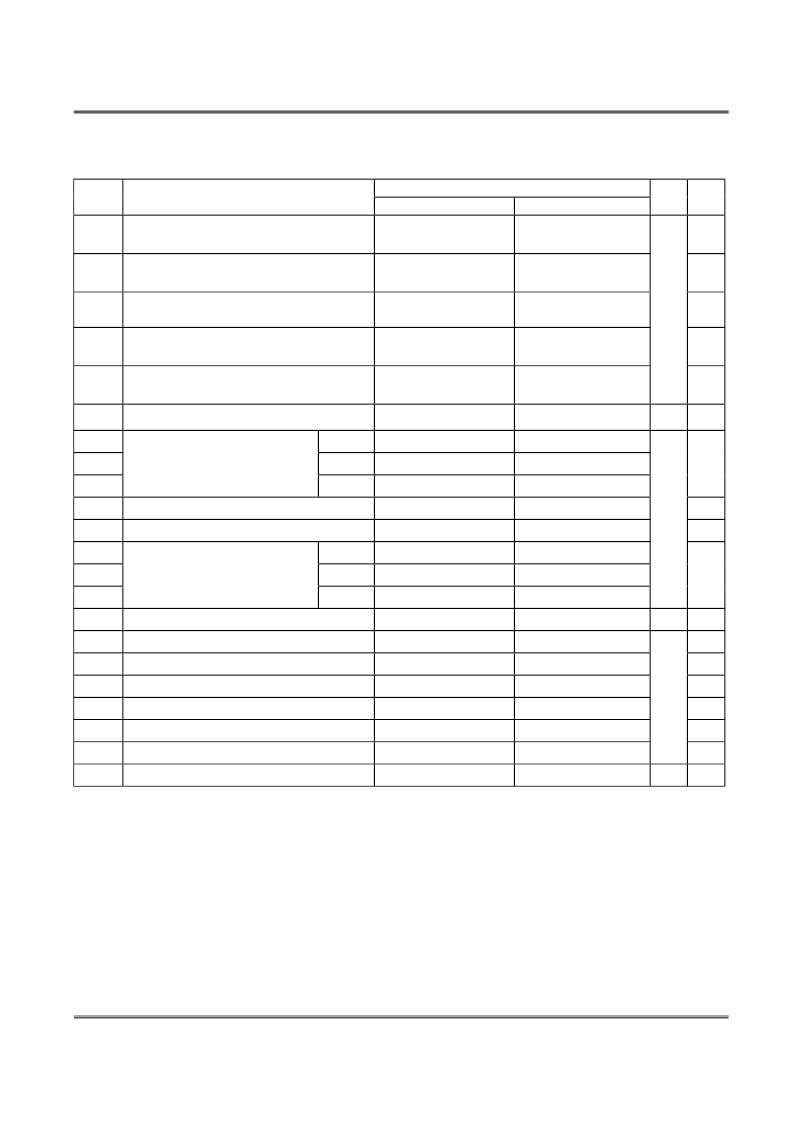
Electrical Characteristics and Recommended A.C. Operating Conditions
(V
DD
= 3.3V
±
0.3V, Ta = -0~70
°
C) (Note: 5, 6, 7, 8)
T431616D/E
TM Technology Inc. reserves the right
P. 19
to change products or specifications without notice.
Publication Date: FEB. 2007
Revision: A
- 5/6/7/7L
Symbol
A.C. Parameter
Min.
Max.
Unit
Note
t
RC
Row cycle time
(same bank)
RAS# to CAS# delay
(same bank)
Precharge to refresh/row activate command
(same bank)
Row activate to row activate delay
(different banks)
Row activate to precharge time
(same bank)
Write recovery time
48/54/63/63
9
t
RCD
15/16/16/16
9
t
RP
15/16/16/16
ns
9
t
RRD
10/12/14/14
9
t
RAS
35/42/42/42
100,000
t
WR
2
Cycle
t
CK1
t
CK2
t
CK3
CL* = 1
-/20/20/20
Clock cycle time
CL* = 2
-/7/8/8
10
CL* = 3
5/6/7/7
t
CH
Clock high time
2/2/2.5/2.5
ns
11
t
CL
Clock low time
2/2/2.5/2.5
11
t
AC1
Access time from CLK
CL* = 1
-/8/13/13
t
AC2
(positive edge)
CL* = 2
-/6/6.5/6.5
11
t
AC3
CL* = 3
4.5/5/5.5/5.5
t
CCD
CAS# to CAS# Delay time
1
Cycle
t
OH
t
LZ
Data output hold time
1.8/2/2/2
10
Data output low impedance
1
t
HZ
Data output high impedance
3/4/5/5
8
t
IS
Data/Address/Control Input set-up time
2
ns
11
t
IH
Data/Address/Control Input hold time
1
11
t
PDE
PowerDown Exit set-up time
2
t
REF
Refresh time
64
ms
* CL is CAS# Latency.
Note:
1. Stress greater than those listed under "Absolute Maximum Ratings" may cause permanent damage to the device.
2. All voltages are referenced to VSS. VIH(Max)=4.6 for pulse width
≤
5ns.VIL(Min)=-1.5Vfor pulse width
≤
5ns.
3. These parameters depend on the cycle rate and these values are measured by the cycle rate under the minimum value of tCK and
tRC. Input signals are changed one time during tCK.
4. These parameters depend on the output loading. Specified values are obtained with the output open.
5.
Power-up sequence is described in Note 12.
6.
A.C. Test Conditions
相关PDF资料 |
PDF描述 |
|---|---|
| T436416A | 4M X 16 SDRAM |
| T436416A-10S | 4M X 16 SDRAM |
| T436416A-10SG | Terminal Block End Barrier; For Use With:AB1 Series Terminal Blocks; Accessory Type:End Barrier; Leaded Process Compatible:Yes; Peak Reflow Compatible (260 C):Yes RoHS Compliant: Yes |
| T436416A-6S | 4M X 16 SDRAM |
| T436416A-6SG | 4M X 16 SDRAM |
相关代理商/技术参数 |
参数描述 |
|---|---|
| T4322 | 制造商:未知厂家 制造商全称:未知厂家 功能描述:TRIANGULAR TYPE |
| T4323 | 制造商:未知厂家 制造商全称:未知厂家 功能描述:TRIANGULAR TYPE |
| T4333 | 制造商:未知厂家 制造商全称:未知厂家 功能描述:TRIANGULAR TYPE |
| T43331G | 制造商:BITECH 制造商全称:Bi technologies 功能描述:Thick Film Super Low Profile SIP Resistor Networks |
| T43331J | 制造商:BITECH 制造商全称:Bi technologies 功能描述:Thick Film Super Low Profile SIP Resistor Networks |
发布紧急采购,3分钟左右您将得到回复。