参数资料
| 型号: | TISP61089BGDR-S |
| 厂商: | Bourns Inc. |
| 文件页数: | 2/20页 |
| 文件大小: | 0K |
| 描述: | PROTECTOR PROGRAMMABLE SLIC |
| 标准包装: | 2,500 |
| 电压 - 击穿: | 64V |
| 电压 - 断路: | 170V |
| 电流 - 峰值脉冲(10 x 1000µs): | 30A |
| 电流 - 保持 (Ih): | 150mA |
| 元件数: | 2 |
| 电容: | 100pF |
| 封装/外壳: | 8-SOIC(0.154",3.90mm 宽) |
| 包装: | 带卷 (TR) |
�� �
�
�TISP61089B� High� Voltage� Ringing� SLIC� Protector�
�Description� (Continued)�
�The� SLIC� line� driver� section� is� typically� powered� from� 0� V� (ground)� and� a� negative� voltage� in� the� region� of� -20� V� to� -150� V.� The� protector� gate� is�
�connected� to� this� negative� supply.� This� references� the� protection� (clipping)� voltage� to� the� negative� supply� voltage.� The� protection� voltage� will�
�then� track� the� negative� supply� voltage� and� the� overvoltage� stress� on� the� SLIC� is� minimized.�
�Positive� overvoltages� are� clipped� to� ground� by� diode� forward� conduction.� Negative� overvoltages� are� initially� clipped� close� to� the� SLIC� negative�
�supply� rail� value.� If� sufficient� current� is� available� from� the� overvoltage,� then� the� protector� SCR� will� switch� into� a� low� voltage� on-state� condition.�
�As� the� overvoltage� subsides,� the� high� holding� current� of� TISP61089B� SCR� helps� prevent� d.c.� latchup.�
�The� TISP61089B� is� intended� to� be� used� with� a� series� combination� of� a� 40� ?� or� higher� resistance� and� a� suitable� overcurrent� protector.� Power�
�fault� compliance� requires� the� series� overcurrent� element� to� open-circuit� or� become� high� impedance� (see� Applications� Information).� For�
�equipment� compliant� to� ITU-T� recommendations� K.20� or� K.21� or� K.45� only,� the� series� resistor� value� is� set� by� the� coordination� requirements.�
�For� coordination� with� a� 400� V� limit� GDT,� a� minimum� series� resistor� value� of� 10� ?� is� recommended.�
�These� monolithic� protection� devices� are� fabricated� in� ion-implanted� planar� vertical� power� structures� for� high� reliability� and� in� normal� system�
�operation� they� are� virtually� transparent.� The� TISP61089B� buffered� gate� design� reduces� the� loading� on� the� SLIC� supply� during� overvoltages�
�caused� by� power� cross� and� induction.� The� TISP61089B� is� available� in� a� 8-pin� plastic� small-outline� surface� mount� package.�
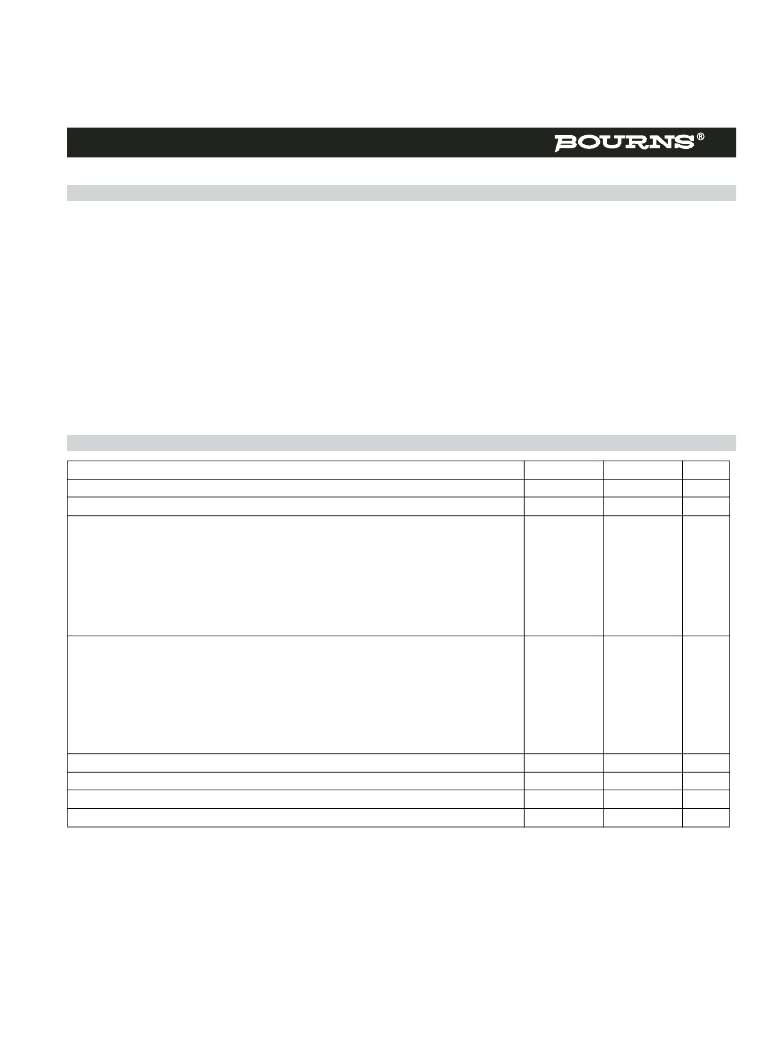
�Absolute� Maximum� Ratings,� -40� °� C� ≤� TJ� ≤� 85� °� C� (Unless� Otherwise� Noted)�
�Rating�
�Repetitive� peak� off-state� voltage,� V� GK� =� 0�
�Repetitive� peak� gate-cathode� voltage,� V� KA� =� 0�
�Symbol�
�V� DRM�
�V� GKRM�
�Value�
�-170�
�-167�
�Unit�
�V�
�V�
�Non-repetitive� peak� on-state� pulse� current� (see� Notes� 1� and� 2)�
�10/1000� μ� s� (Telcordia� (Bellcore)� GR-1089-CORE,� Issue� 2,� February� 1999,� Section� 4)�
�5/320� μ� s� (ITU-T� K.20,� K.21&� K.45,� K.44� open-circuit� voltage� wave� shape� 10/700� μ� s)�
�30�
�40�
�10/360� μ� s� (Telcordia� (Bellcore)� GR-1089-CORE,� Issue� 2,� February� 1999,� Section� 4)�
�1.2/50� μ� s� (Telcordia� (Bellcore)� GR-1089-CORE,� Issue� 2,� February� 1999,� Section� 4)�
�2/10� μ� s� (Telcordia� (Bellcore)� GR-1089-CORE,� Issue� 2,� February� 1999,�
�Section� 4)�
�T� J� =� 25� °� C�
�I� TSP�
�40�
�100�
�120�
�170�
�A�
�Non-repetitive� peak� on-state� current,� 60� Hz� (see� Notes� 1,� 2� and� 3)�
�0.5� s�
�1s�
�6.5�
�4.6�
�2s�
�5s�
�30� s�
�900� s�
�Non-repetitive� peak� gate� current,� 1/2� μ� s� pulse,� cathodes� commoned� (see� Notes� 1� and� 2)�
�Operating� free-air� temperature� range�
�Junction� temperature�
�Storage temperature range�
�I� TSM�
�I� GSM�
�T� A�
�T� J�
�T� stg�
�3.4�
�2.3�
�1.3�
�0.73�
�+40�
�-40� to� +85�
�-40� to� +150�
�-40 to +150�
�A�
�A�
�°� C�
�°� C�
�°C�
�NOTES:� 1.� Initially,� the� protector� must� be� in� thermal� equilibrium� with� -40� °� C� ≤� T� J� ≤� 85� °� C.� The� surge� may� be� repeated� after� the� device� returns�
�to� its� initial� conditions.�
�2.� The� rated� current� values� may� be� applied� either� to� the� Ring� to� Ground� or� to� the� Tip� to� Ground� terminal� pairs.� Additionally,� both�
�terminal� pairs� may� have� their� rated� current� values� applied� simultaneously� (in� this� case� the� Ground� terminal� current� will� be� twice�
�the� rated� current� value� of� an� individual� terminal� pair).� Above� 85� °� C,� derate� linearly� to� zero� at� 150� °� C� lead� temperature.�
�3.� Values� for� V� GG� =� -100� V.� For� values� at� other� voltages� see� Figure� 2.�
�OCTOBER� 2000� -� REVISED� JULY� 2008�
�Specifications� are� subject� to� change� without� notice.�
�Customers� should� verify� actual� device� performance� in� their� specific� applications.�
�相关PDF资料 |
PDF描述 |
|---|---|
| 1-1586585-0 | CONN HEADER 10POS VERT 4.2MM TIN |
| 641216-3 | CONN HEADER RT/A .100 3POS 30AU |
| 103233-1 | CONN HDR 4POS A/PIN STR PCB |
| 929975-01-28-RK | CONN RECEPT .100 DUAL STR 56POS |
| 929850-01-30-10 | CONN RECEPT .100 SNGL STR 30POS |
相关代理商/技术参数 |
参数描述 |
|---|---|
| TISP61089BSDR-S | 功能描述:SCR PROTECTOR - QUAD PROGRAMMABLE RoHS:否 制造商:STMicroelectronics 最大转折电流 IBO:480 A 额定重复关闭状态电压 VDRM:600 V 关闭状态漏泄电流(在 VDRM IDRM 下):5 uA 开启状态 RMS 电流 (It RMS): 正向电压下降:1.6 V 栅触发电压 (Vgt):1.3 V 最大栅极峰值反向电压:5 V 栅触发电流 (Igt):35 mA 保持电流(Ih 最大值):75 mA 安装风格:Through Hole 封装 / 箱体:TO-220 封装:Tube |
| TISP61089D | 功能描述:SCR Dual P Gate Forward Conducting RoHS:否 制造商:STMicroelectronics 最大转折电流 IBO:480 A 额定重复关闭状态电压 VDRM:600 V 关闭状态漏泄电流(在 VDRM IDRM 下):5 uA 开启状态 RMS 电流 (It RMS): 正向电压下降:1.6 V 栅触发电压 (Vgt):1.3 V 最大栅极峰值反向电压:5 V 栅触发电流 (Igt):35 mA 保持电流(Ih 最大值):75 mA 安装风格:Through Hole 封装 / 箱体:TO-220 封装:Tube |
| TISP61089DR | 功能描述:SCR Dual P Gate Forward Conducting RoHS:否 制造商:STMicroelectronics 最大转折电流 IBO:480 A 额定重复关闭状态电压 VDRM:600 V 关闭状态漏泄电流(在 VDRM IDRM 下):5 uA 开启状态 RMS 电流 (It RMS): 正向电压下降:1.6 V 栅触发电压 (Vgt):1.3 V 最大栅极峰值反向电压:5 V 栅触发电流 (Igt):35 mA 保持电流(Ih 最大值):75 mA 安装风格:Through Hole 封装 / 箱体:TO-220 封装:Tube |
| TISP61089DR-S | 功能描述:SCR Dual P Gate Forward Conducting RoHS:否 制造商:STMicroelectronics 最大转折电流 IBO:480 A 额定重复关闭状态电压 VDRM:600 V 关闭状态漏泄电流(在 VDRM IDRM 下):5 uA 开启状态 RMS 电流 (It RMS): 正向电压下降:1.6 V 栅触发电压 (Vgt):1.3 V 最大栅极峰值反向电压:5 V 栅触发电流 (Igt):35 mA 保持电流(Ih 最大值):75 mA 安装风格:Through Hole 封装 / 箱体:TO-220 封装:Tube |
| TISP61089DS | 制造商:Bourns Inc 功能描述: |
发布紧急采购,3分钟左右您将得到回复。