参数资料
| 型号: | TISP61089BGDR-S |
| 厂商: | Bourns Inc. |
| 文件页数: | 6/20页 |
| 文件大小: | 0K |
| 描述: | PROTECTOR PROGRAMMABLE SLIC |
| 标准包装: | 2,500 |
| 电压 - 击穿: | 64V |
| 电压 - 断路: | 170V |
| 电流 - 峰值脉冲(10 x 1000µs): | 30A |
| 电流 - 保持 (Ih): | 150mA |
| 元件数: | 2 |
| 电容: | 100pF |
| 封装/外壳: | 8-SOIC(0.154",3.90mm 宽) |
| 包装: | 带卷 (TR) |
�� �
�
�TISP61089B� High� Voltage� Ringing� SLIC� Protector�
�APPLICATIONS� INFORMATION�
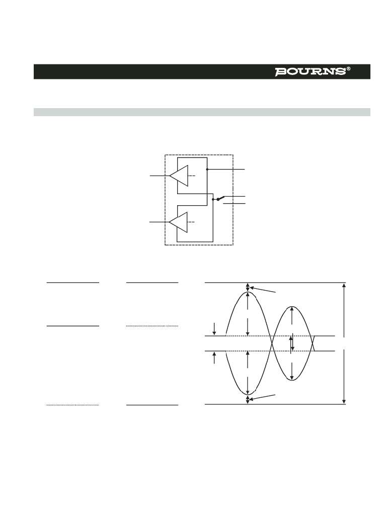
�Operation� of� Ringing� SLICs� using� Multiple� Negative� Voltage� Supply� Rails�
�Figure� 4� shows� a� typical� powering� arrangement� for� a� multi-supply� rail� SLIC.� VBATL� is� a� lower� (smaller)� voltage� supply� than� VBATH.� With� supply�
�switch� S1� in� the� position� shown,� the� line� driver� amplifiers� are� powered� between� 0� V� and� VBATL.� This� mode� minimizes� the� power� consumption�
�for� short� loop� transmission.� For� long� loops� and� to� generate� ringing,� the� driver� voltage� is� increased� by� operating� S1� to� connect� VBATH.� These�
�conditions� are� shown� in� Figure� 5.�
�SLIC�
�0V�
�LINE�
�LINE�
�S1�
�SUPPLY�
�V� BATL�
�V� BATH�
�DRIVERS�
�SWITCH�
�AI6XCC�
�Figure� 4.� SLIC� with� Voltage� Supply� Switching�
�0V�
�0V�
�V� PKRING� /2�
�V� SLICG�
�0V�
�V� BATL�
�V� BATH�
�V� DCRING�
�V� PKRING� /2�
�V� PKRING� /2�
�V� PKRING� /2�
�V� SLICH�
�V� BATH�
�V� BATH�
�SHORT� LOOP�
�LONG� LOOP�
�RINGING�
�AI6XCD�
�Figure� 5.� Driver� Supply� Voltage� Levels�
�Conventional� ringing� is� typically� unbalanced� ground� or� battery� backed.� To� minimize� the� supply� voltage� required,� most� multi-rail� SLICs� use�
�balanced� ringing� as� shown� in� Figure� 5.� The� ringing� has� d.c.,� V� DCRING� ,� and� a.c.,� V� PKRING� ,� components.� A� 70� V� r.m.s.� a.c.� sinusoidal� ring� signal�
�has� a� peak� value,� V� PKRING� ,� of� 99� V.� If� the� d.c.� component� was� 20� V,� then� the� total� voltage� swing� needed� would� be� 99� +� 20� =� 119� V.� There� are�
�internal� losses� in� the� SLIC� from� ground,� V� SLICG� ,� and� the� negative� supply,� V� SLICH� .� The� sum� of� these� two� losses� generally� amounts� to� a� total� of�
�10� V.� This� makes� a� total,� V� BATH� ,� supply� rail� value� of� 119� +� 10� =� 129� V.�
�In� some� cases� a� trapezoidal� a.c.� ring� signal� is� used.� This� would� have� a� peak� to� r.m.s� ratio� (crest� factor)� of� about� 1.25,� increasing� the� r.m.s.� a.c.�
�ring� level� by� 13� %.� The� d.c.� ring� voltage� may� be� lowered� for� short� loop� applications.�
�OCTOBER� 2000� -� REVISED� JULY� 2008�
�Specifications� are� subject� to� change� without� notice.�
�Customers� should� verify� actual� device� performance� in� their� specific� applications.�
�相关PDF资料 |
PDF描述 |
|---|---|
| 1-1586585-0 | CONN HEADER 10POS VERT 4.2MM TIN |
| 641216-3 | CONN HEADER RT/A .100 3POS 30AU |
| 103233-1 | CONN HDR 4POS A/PIN STR PCB |
| 929975-01-28-RK | CONN RECEPT .100 DUAL STR 56POS |
| 929850-01-30-10 | CONN RECEPT .100 SNGL STR 30POS |
相关代理商/技术参数 |
参数描述 |
|---|---|
| TISP61089BSDR-S | 功能描述:SCR PROTECTOR - QUAD PROGRAMMABLE RoHS:否 制造商:STMicroelectronics 最大转折电流 IBO:480 A 额定重复关闭状态电压 VDRM:600 V 关闭状态漏泄电流(在 VDRM IDRM 下):5 uA 开启状态 RMS 电流 (It RMS): 正向电压下降:1.6 V 栅触发电压 (Vgt):1.3 V 最大栅极峰值反向电压:5 V 栅触发电流 (Igt):35 mA 保持电流(Ih 最大值):75 mA 安装风格:Through Hole 封装 / 箱体:TO-220 封装:Tube |
| TISP61089D | 功能描述:SCR Dual P Gate Forward Conducting RoHS:否 制造商:STMicroelectronics 最大转折电流 IBO:480 A 额定重复关闭状态电压 VDRM:600 V 关闭状态漏泄电流(在 VDRM IDRM 下):5 uA 开启状态 RMS 电流 (It RMS): 正向电压下降:1.6 V 栅触发电压 (Vgt):1.3 V 最大栅极峰值反向电压:5 V 栅触发电流 (Igt):35 mA 保持电流(Ih 最大值):75 mA 安装风格:Through Hole 封装 / 箱体:TO-220 封装:Tube |
| TISP61089DR | 功能描述:SCR Dual P Gate Forward Conducting RoHS:否 制造商:STMicroelectronics 最大转折电流 IBO:480 A 额定重复关闭状态电压 VDRM:600 V 关闭状态漏泄电流(在 VDRM IDRM 下):5 uA 开启状态 RMS 电流 (It RMS): 正向电压下降:1.6 V 栅触发电压 (Vgt):1.3 V 最大栅极峰值反向电压:5 V 栅触发电流 (Igt):35 mA 保持电流(Ih 最大值):75 mA 安装风格:Through Hole 封装 / 箱体:TO-220 封装:Tube |
| TISP61089DR-S | 功能描述:SCR Dual P Gate Forward Conducting RoHS:否 制造商:STMicroelectronics 最大转折电流 IBO:480 A 额定重复关闭状态电压 VDRM:600 V 关闭状态漏泄电流(在 VDRM IDRM 下):5 uA 开启状态 RMS 电流 (It RMS): 正向电压下降:1.6 V 栅触发电压 (Vgt):1.3 V 最大栅极峰值反向电压:5 V 栅触发电流 (Igt):35 mA 保持电流(Ih 最大值):75 mA 安装风格:Through Hole 封装 / 箱体:TO-220 封装:Tube |
| TISP61089DS | 制造商:Bourns Inc 功能描述: |
发布紧急采购,3分钟左右您将得到回复。