- 您现在的位置:买卖IC网 > PDF目录68418 > TLC320AD50IDWR (TEXAS INSTRUMENTS INC) SPECIALTY ANALOG CIRCUIT, PDSO28 PDF资料下载
参数资料
| 型号: | TLC320AD50IDWR |
| 厂商: | TEXAS INSTRUMENTS INC |
| 元件分类: | 模拟信号调理 |
| 英文描述: | SPECIALTY ANALOG CIRCUIT, PDSO28 |
| 封装: | PLASTIC, SO-28 |
| 文件页数: | 14/55页 |
| 文件大小: | 506K |
| 代理商: | TLC320AD50IDWR |
第1页第2页第3页第4页第5页第6页第7页第8页第9页第10页第11页第12页第13页当前第14页第15页第16页第17页第18页第19页第20页第21页第22页第23页第24页第25页第26页第27页第28页第29页第30页第31页第32页第33页第34页第35页第36页第37页第38页第39页第40页第41页第42页第43页第44页第45页第46页第47页第48页第49页第50页第51页第52页第53页第54页第55页
2–6
2.2
Reset and Power-Down Functions
2.2.1
Software and Hardware Reset
The TLC320AD50C and TLC320AD52C reset the internal counters and registers in response to either of two events:
1.
A low-going reset pulse is applied to terminal RESET.
2.
A 1 is written to the programmable software reset bit (D7 of control register 1).
Either event resets the control registers and clears all the sequential circuits in the device. Reset signals should be
at least 6 master clock periods long.
After hardware reset, the default contents of all registers is 0.
After a hardware or software reset, the AD50 and AD52 require a finite amount of time for the internal PLL to stabilize.
During this time, no control words or D/A data should be written to the device.
The reset sequence should be as follows:
1.
Assert reset (pulse width encompassing at least 6 MCLK periods)
2.
Deactivate reset
3.
Wait for SCLKS to be generated by the master device. This will take approximately 100
s.
4.
Wait for 18 frame syncs to occur
5.
Write control and configuration data
6.
Collect conversion data
2.2.2
Software and Hardware Power Down
Except for the digital interface, most of the device enters the power-down mode when D6 in control 1 register is set
to 1. When PWRDWN is taken low, the entire device is powered down. In either case, the register contents are
preserved and the output of the monitor amplifier is held at the midpoint voltage to minimize pops and clicks.
The amount of power drawn during software power down is higher than it is during a hardware power down because
of the current required to keep the digital interface active. Additional differences between software and hardware
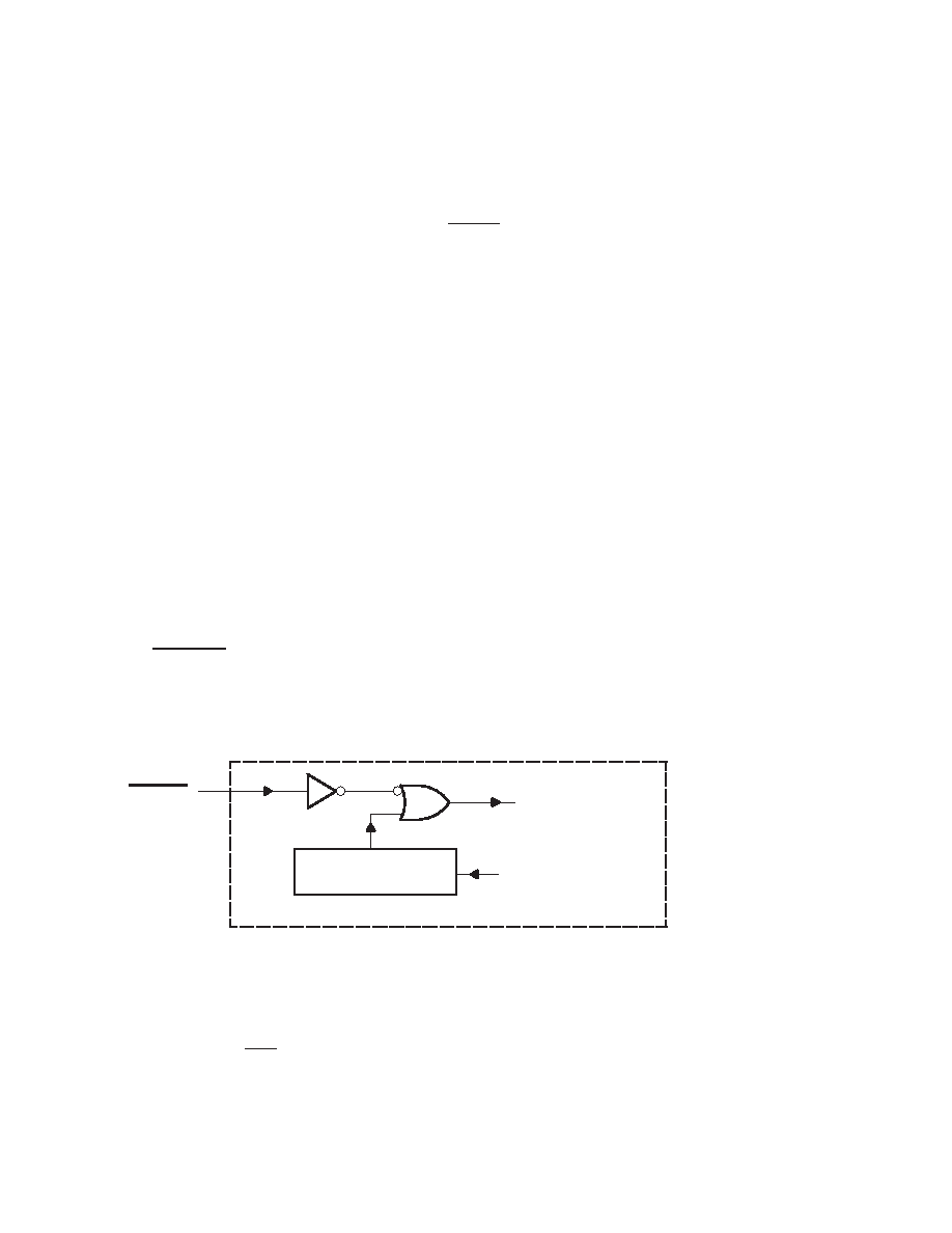
power-down modes are detailed in the following paragraphs. Figure 2–7 represents the internal power-down logic.
PWRDWN
D6 is Programmed
Through a Secondary
Write Operation
Software Power Down
(Control Register 1, D6)
Internal TLC320AD50C
Figure 2–7. Internal Power-Down Logic
2.2.2.1 Software Power Down
When D6 of control 1 register is set to 1, the device enters the software power-down mode. In this state, the digital
interface circuit is still active while the internal ADC and DAC channels and differential outputs OUTP and OUTM are
disabled, and DOUT and FSD are inactive. Register data in the secondary serial communications is still accepted,
but data in the primary serial communications is ignored. The device returns to normal operation when D6 of control
1 register is reset to 0.
相关PDF资料 |
PDF描述 |
|---|---|
| TLE4935-2LS | SPECIALTY ANALOG CIRCUIT, PSIP3 |
| TLE4905LS | SPECIALTY ANALOG CIRCUIT, PSIP3 |
| TLE4935LS | SPECIALTY ANALOG CIRCUIT, PSIP3 |
| TPD3F303DQDR | SPECIALTY ANALOG CIRCUIT, PDSO8 |
| TPS2010DR | 1-CHANNEL POWER SUPPLY SUPPORT CKT, PDSO8 |
相关代理商/技术参数 |
参数描述 |
|---|---|
| TLC320AD50IPT | 制造商:TI 制造商全称:Texas Instruments 功能描述:SIGMA-DELTA ANALOG INTERFACE CIRCUITS WITH MASTER-SLAVE FUNCTION |
| TLC320AD52CDW | 制造商:TI 制造商全称:Texas Instruments 功能描述:SIGMA-DELTA ANALOG INTERFACE CIRCUITS WITH MASTER-SLAVE FUNCTION |
| TLC320AD52CPT | 功能描述:IC ANALOG INTERFACE W/MS 48-LQFP RoHS:否 类别:集成电路 (IC) >> 接口 - 编解码器 系列:- 标准包装:2,500 系列:- 类型:PCM 数据接口:PCM 音频接口 分辨率(位):15 b ADC / DAC 数量:1 / 1 三角积分调变:是 S/N 比,标准 ADC / DAC (db):- 动态范围,标准 ADC / DAC (db):- 电压 - 电源,模拟:2.7 V ~ 3.3 V 电压 - 电源,数字:2.7 V ~ 3.3 V 工作温度:-40°C ~ 85°C 安装类型:表面贴装 封装/外壳:80-VFBGA 供应商设备封装:80-BGA MICROSTAR JUNIOR(5x5) 包装:带卷 (TR) 其它名称:296-21257-2 |
| TLC320AD535 | 制造商:TI 制造商全称:Texas Instruments 功能描述:DUAL CHANNEL VOICE/DATA CODEC |
| TLC320AD535C | 制造商:TI 制造商全称:Texas Instruments 功能描述:DUAL CHANNEL VOICE/DATA CODEC |
发布紧急采购,3分钟左右您将得到回复。