- 您现在的位置:买卖IC网 > PDF目录68418 > TLC320AD50IDWR (TEXAS INSTRUMENTS INC) SPECIALTY ANALOG CIRCUIT, PDSO28 PDF资料下载
参数资料
| 型号: | TLC320AD50IDWR |
| 厂商: | TEXAS INSTRUMENTS INC |
| 元件分类: | 模拟信号调理 |
| 英文描述: | SPECIALTY ANALOG CIRCUIT, PDSO28 |
| 封装: | PLASTIC, SO-28 |
| 文件页数: | 4/55页 |
| 文件大小: | 506K |
| 代理商: | TLC320AD50IDWR |
第1页第2页第3页当前第4页第5页第6页第7页第8页第9页第10页第11页第12页第13页第14页第15页第16页第17页第18页第19页第20页第21页第22页第23页第24页第25页第26页第27页第28页第29页第30页第31页第32页第33页第34页第35页第36页第37页第38页第39页第40页第41页第42页第43页第44页第45页第46页第47页第48页第49页第50页第51页第52页第53页第54页第55页
1–5
1.5
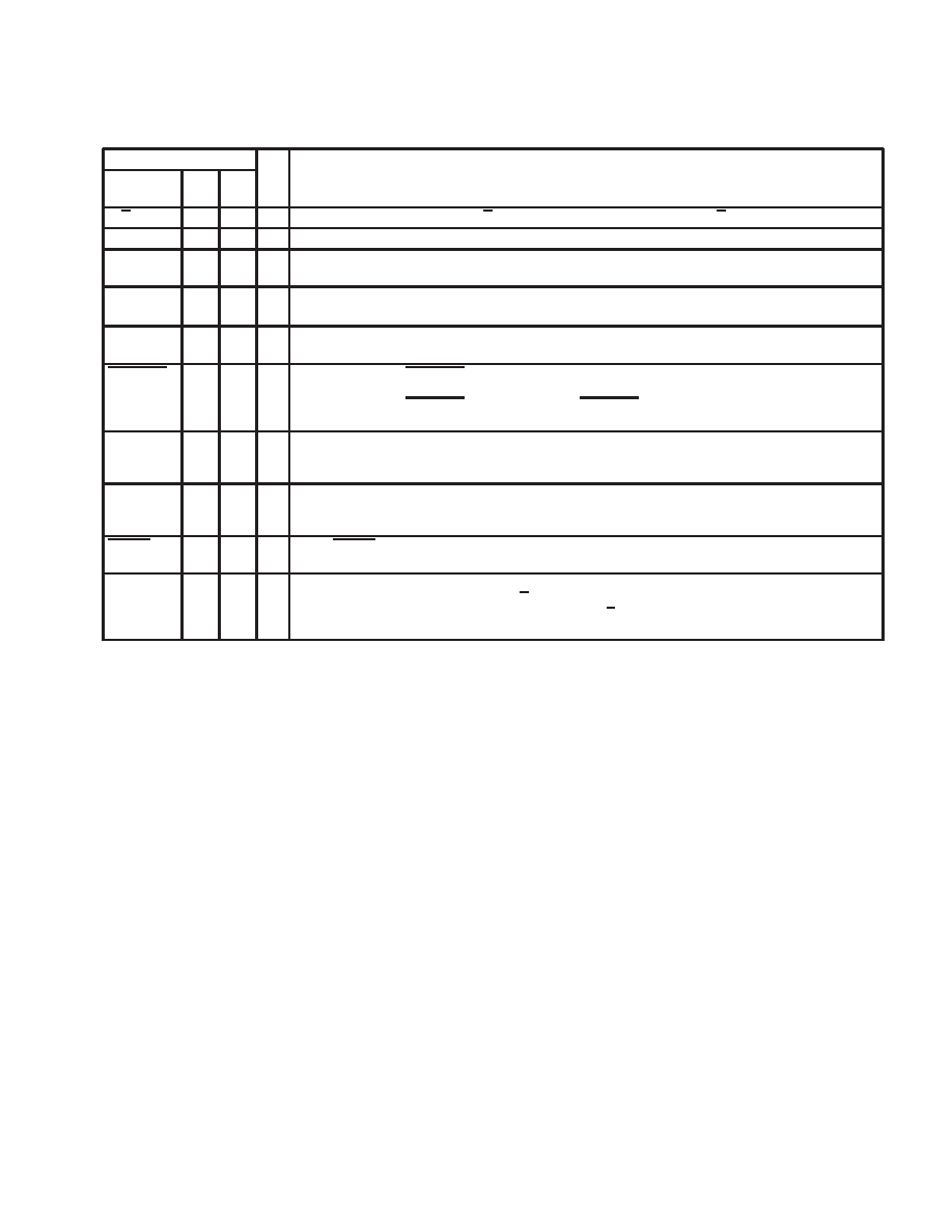
Terminal Functions (Continued)
TERMINAL
NAME
NO.
PT
NO.
DW
I/O
DESCRIPTION
M/S
29
22
I
Master/slave select input. When M/S is high, the device is the master. When M/S is low, the device is a slave.
MCLK
25
18
I
Master clock. MCLK derives the internal clocks of the sigma-delta analog interface circuit.
MONOUT
40
27
O
Monitor output. MONOUT allows for monitoring of the analog input and is a high-impedance output. The gain
or mute is selected using control 1 register.
OUTM
36
24
O
Inverting output of the DAC. The OUTM output can be loaded with 600
. OUTM is functionally identical with
and complementary to OUTP. OUTM can also be used alone for single-ended operation.
OUTP
35
23
O
Noninverting output of the DAC. The OUTP output can be loaded with 600
. OUTP can also be used alone
for single-ended operation.
PWRDWN
22
16
I
Power down. When PWRDWN is pulled low, the device goes into a power-down mode, the serial interface
is disabled. However, all the register values are sustained and the device resumes full power operation without
reinitialization when PWRDWN is pulled high again. PWRDWN resets the counters only and preserves the
programmed register contents (see paragraph 2.2.2 for more information).
REFM
46
2
O
Voltage reference filter output. REFM is provided for low-pass filtering of the internal bandgap reference. The
optimal ceramic capacitor value is 0.1
F and should be connected between REFM and REFP. DC voltage
at REFM is 0 V.
REFP
45
1
O
Voltage reference filter positive output. REFP is provided for low-pass filtering of the internal bandgap
reference. The optimal ceramic capacitor value is 0.1
F and should be connected between REFP and REFM.
DC voltage at REFP is 3.2 V.
RESET
21
15
I
Reset. RESET initializes all of the internal registers to their default values. The serial port can be configured
to the default state accordingly. See section 6 and paragraph 2.2.1 for more information.
SCLK
26
19
I/O
Shift clock. The SCLK signal clocks serial data in through DIN and out through DOUT during the frame-sync
interval. When configured as an output (M/S high), SCLK is generated internally by multiplying the frame-sync
signal frequency by 256. When configured as an input (M/S low), SCLK is generated externally and must be
synchronous with the master clock and frame sync.
NOTES:
1. Separate analog and digital power and ground pins are supplied on this device. For best operation and results, the PC board designer
should utilize separate analog and digital power supplies as well as separate analog and digital ground planes.
2. All digital inputs and outputs are TTL compatible, unless otherwise noted (for DVDD = 5 V).
相关PDF资料 |
PDF描述 |
|---|---|
| TLE4935-2LS | SPECIALTY ANALOG CIRCUIT, PSIP3 |
| TLE4905LS | SPECIALTY ANALOG CIRCUIT, PSIP3 |
| TLE4935LS | SPECIALTY ANALOG CIRCUIT, PSIP3 |
| TPD3F303DQDR | SPECIALTY ANALOG CIRCUIT, PDSO8 |
| TPS2010DR | 1-CHANNEL POWER SUPPLY SUPPORT CKT, PDSO8 |
相关代理商/技术参数 |
参数描述 |
|---|---|
| TLC320AD50IPT | 制造商:TI 制造商全称:Texas Instruments 功能描述:SIGMA-DELTA ANALOG INTERFACE CIRCUITS WITH MASTER-SLAVE FUNCTION |
| TLC320AD52CDW | 制造商:TI 制造商全称:Texas Instruments 功能描述:SIGMA-DELTA ANALOG INTERFACE CIRCUITS WITH MASTER-SLAVE FUNCTION |
| TLC320AD52CPT | 功能描述:IC ANALOG INTERFACE W/MS 48-LQFP RoHS:否 类别:集成电路 (IC) >> 接口 - 编解码器 系列:- 标准包装:2,500 系列:- 类型:PCM 数据接口:PCM 音频接口 分辨率(位):15 b ADC / DAC 数量:1 / 1 三角积分调变:是 S/N 比,标准 ADC / DAC (db):- 动态范围,标准 ADC / DAC (db):- 电压 - 电源,模拟:2.7 V ~ 3.3 V 电压 - 电源,数字:2.7 V ~ 3.3 V 工作温度:-40°C ~ 85°C 安装类型:表面贴装 封装/外壳:80-VFBGA 供应商设备封装:80-BGA MICROSTAR JUNIOR(5x5) 包装:带卷 (TR) 其它名称:296-21257-2 |
| TLC320AD535 | 制造商:TI 制造商全称:Texas Instruments 功能描述:DUAL CHANNEL VOICE/DATA CODEC |
| TLC320AD535C | 制造商:TI 制造商全称:Texas Instruments 功能描述:DUAL CHANNEL VOICE/DATA CODEC |
发布紧急采购,3分钟左右您将得到回复。