- 您现在的位置:买卖IC网 > Datasheet目录1011 > TMPSNS-RTD1 (Microchip Technology)BOARD EVAL PT100 RTD TEMP SENSOR Datasheet资料下载
参数资料
| 型号: | TMPSNS-RTD1 |
| 厂商: | Microchip Technology |
| 文件页数: | 17/43页 |
| 文件大小: | 0K |
| 描述: | BOARD EVAL PT100 RTD TEMP SENSOR |
| 标准包装: | 1 |
| 传感器类型: | 温度 |
| 接口: | USB |
| 嵌入式: | 是,MCU,8 位 |
| 已供物品: | 板,缆线,CD |
| 已用 IC / 零件: | MCP3301,MCP6S26,PIC18F2550 |
| 产品目录页面: | 672 (CN2011-ZH PDF) |
| 相关产品: | MCP3301T-BI/SN-ND - IC ADC 13BIT 2.7V 1CH SPI 8-SOIC MCP3301-BI/SN-ND - IC ADC 13BIT 2.7V SPI 8-SOIC MCP3301T-CI/SN-ND - IC ADC 13BIT 2.7V 1CH SPI 8-SOIC MCP3301T-BI/MS-ND - IC ADC 13BIT 2.7V 1CH SPI 8-MSOP MCP3301T-CI/MS-ND - IC ADC 13BIT 2.7V 1CH SPI 8-MSOP MCP3301-BI/P-ND - IC ADC 13BIT 2.7V SPI 8-DIP MCP3301-BI/MS-ND - IC ADC 13BIT 2.7V SPI 8-MSOP MCP3301-CI/SN-ND - IC ADC 13BIT 2.7V 1CH SPI 8SOIC MCP3301-CI/P-ND - IC ADC 13BIT 2.7V 1CH SPI 8-DIP MCP3301-CI/MS-ND - IC ADC 13BIT 2.7V 1CH SPI 8-MSOP |
第1页第2页第3页第4页第5页第6页第7页第8页第9页第10页第11页第12页第13页第14页第15页第16页当前第17页第18页第19页第20页第21页第22页第23页第24页第25页第26页第27页第28页第29页第30页第31页第32页第33页第34页第35页第36页第37页第38页第39页第40页第41页第42页第43页
�� �
�
�MCP6S21/2/6/8�
�4.2.2�
�RAIL-TO-RAIL� INPUT�
�4.3�
�Resistor� Ladder�
�The� input� stage� of� the� internal� op� amp� uses� two� differ-�
�ential� input� stages� in� parallel;� one� operates� at� low� V� IN�
�(input� voltage),� while� the� other� operates� at� high� V� IN� .�
�With� this� topology,� the� internal� inputs� can� operate� to�
�0.3V� past� either� supply� rail.� The� input� offset� voltage� is�
�measured� at� both� V� IN� =� V� SS� -� 0.3V� and� V� DD� +� 0.3V� to�
�ensure� proper� operation.�
�The� transition� between� the� two� input� stages� occurs�
�when� V� IN� ≈� V� DD� -� 1.5V.� For� the� best� distortion� and� gain�
�linearity,� avoid� this� region� of� operation.�
�The� resistor� ladder� shown� in� Figure� 4-1� (R� LAD� =� R� F� +�
�R� G� )� sets� the� gain.� Placing� the� gain� switches� in� series�
�with� the� inverting� input� reduces� the� parasitic� capaci-�
�tance,� distortion� and� gain� mismatch.�
�R� LAD� is� an� additional� load� on� the� output� of� the� PGA� and�
�causes� additional� current� draw� from� the� supplies.�
�In� Shutdown� mode,� R� LAD� is� still� attached� to� the� OUT�
�and� V� REF� pins.� Thus,� these� pins� and� the� internal� ampli-�
�fier� ’s� inverting� input� are� all� connected� through� R� LAD�
�and� the� output� is� not� high-Z� (unlike� the� external� op�
�4.2.3�
�RAIL-TO-RAIL� OUTPUT�
�amp).�
�The� Maximum� Output� Voltage� Swing� is� the� maximum�
�swing� possible� under� a� particular� output� load.� Accord-�
�ing� to� the� specification� table,� the� output� can� reach�
�within� 60� mV� of� either� supply� rail� when� R� L� =� 10� k� ?� and�
�V� REF� =� V� DD� /2.� See� Figure� 2-21� for� typical� performance�
�under� other� conditions.�
�While� R� LAD� contributes� to� the� output� noise,� its� effect� is�
��4.4� Shutdown� Mode�
�These� PGAs� use� a� software� shutdown� command.�
�When� the� SPI� interface� sends� a� shutdown� command,�
�the� internal� op� amp� is� shut� down� and� its� output� placed�
�4.2.4�
�INPUT� VOLTAGE� AND� PHASE�
�in� a� high-Z� state.�
�REVERSAL�
�The� amplifier� family� is� designed� with� CMOS� input�
�devices.� It� is� designed� to� not� exhibit� phase� inversion�
�when� the� input� pins� exceed� the� supply� voltages.�
��supplies� with� no� resulting� phase� inversion.�
�The� maximum� voltage� that� can� be� applied� to� the� input�
�pins� (CHX)� is� V� SS� -� 0.3V� to� V� DD� +� 0.3V.� Voltages� on� the�
�inputs� that� exceed� this� absolute� maximum� rating� can�
�cause� excessive� current� to� flow� in� or� out� of� the� input�
�pins.� Current� beyond� ±2� mA� can� cause� possible� reli-�
�ability� problems.� Applications� that� exceed� this� rating�
�must� be� externally� limited� with� an� input� resistor,� as�
��R� IN� CHX�
�The� resistive� ladder� is� always� connected� between�
�V� REF� and� V� OUT� ;� even� in� shutdown.� This� means� that� the�
�output� resistance� will� be� on� the� order� of� 5� k� ?� and� there�
�will� be� a� path� for� output� signals� to� appear� at� the� input.�
�The� Power-on� Reset� (POR)� circuitry� will� temporarily�
�place� the� part� in� shutdown� when� activated.� See�
��R� IN� ≥� -------------------------------------------------------------------------------�
�V� SS� –� (� Minimum� expected� V� IN� )�
�R� IN� ≥� ----------------------------------------------------------------------------�
�V� IN�
�MCP6S2X�
�(� Maximum� expected� V� IN� )� –� V� DD�
�2� mA�
�2� mA�
�V� OUT�
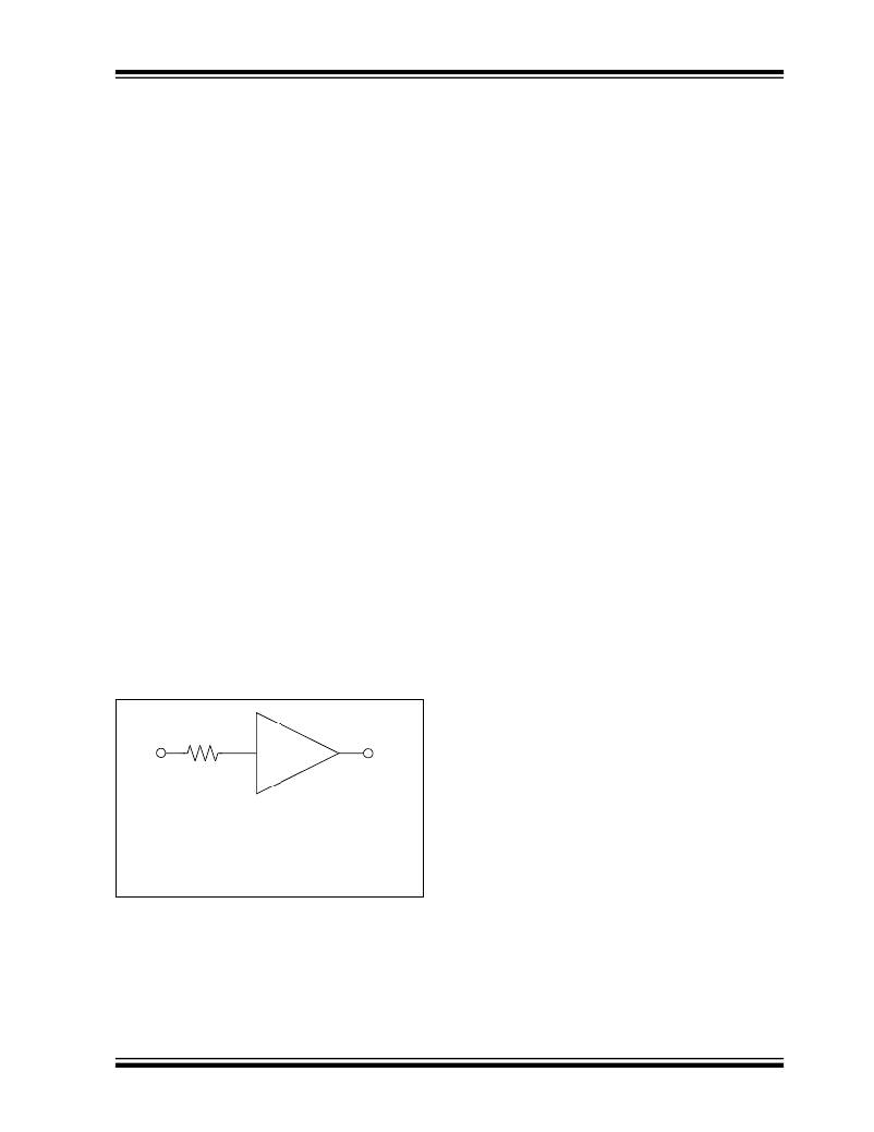
�FIGURE� 4-2:�
�into� an� input� pin.�
�R� IN� limits� the� current� flow�
�?� 2003� Microchip� Technology� Inc.�
�DS21117A-page� 17�
�相关PDF资料 |
PDF描述 |
|---|---|
| 30700-5080 | 汽车连接器 HDAC64 DR RA HDR 8 C HDR 8 CKT GRAY POL 1 |
| TMS-CCUV-SLEEVE-10-X-32MM | HEAT SHRINK SLEEVE |
| TMW-.255X1.70-YELLOW-BOX | HEAT SHRINK TMW .255 YL 1.70 IN |
| TMW.330-1.85" | HEAT SHRINK TMW .330 PK 1.85 IN |
| DB0805A2650AWTR\500 | 信号调节 Directional Coupler 2650 MHz +/- 50 |
相关代理商/技术参数 |
参数描述 |
|---|---|
| TMPT2369ALT | 制造商:ALL 功能描述:ALLEGRO NXC7D |
| TMPT2SU1 | 制造商:Red Lion Controls 功能描述:THERMOCOUPLE TEMP PROBE, TYPE T, 400?F 制造商:Red Lion Controls 功能描述:TYPE T 400DEG F |
| TMPT3906LT | 制造商:ALL 功能描述:ALLEGRO S9K3A |
| TMPT5089LT | 制造商:Allegro MicroSystems LLC 功能描述:Bipolar Junction Transistor, NPN Type, TO-236 |
| TMPTQD01 | 制造商:Red Lion Controls 功能描述:TC PROBE, QUICK DISCON TYPE T SST .062 制造商:Red Lion Controls 功能描述:QUICK DISCONNECT MINI TYPE T |
发布紧急采购,3分钟左右您将得到回复。