- 您现在的位置:买卖IC网 > PDF目录69503 > TPS23756PWP (TEXAS INSTRUMENTS INC) 1.1 A SWITCHING CONTROLLER, 278 kHz SWITCHING FREQ-MAX, PDSO20 PDF资料下载
参数资料
| 型号: | TPS23756PWP |
| 厂商: | TEXAS INSTRUMENTS INC |
| 元件分类: | 稳压器 |
| 英文描述: | 1.1 A SWITCHING CONTROLLER, 278 kHz SWITCHING FREQ-MAX, PDSO20 |
| 封装: | GREEN, PLASTIC, HTSSOP-20 |
| 文件页数: | 13/41页 |
| 文件大小: | 1405K |
| 代理商: | TPS23756PWP |
第1页第2页第3页第4页第5页第6页第7页第8页第9页第10页第11页第12页当前第13页第14页第15页第16页第17页第18页第19页第20页第21页第22页第23页第24页第25页第26页第27页第28页第29页第30页第31页第32页第33页第34页第35页第36页第37页第38页第39页第40页第41页
1
3
4
6
8
9
10
t-Time-10ms/div
IPI
V DD-RTN
V C-RTN
Inrush
VOUT
PIPowered
Switchingstarts
T2P @output
9
0
1
2
3
4
5
6
7
8
5V/div
200mA/div
10V/div
2V/div
50V/div
TPS23754
TPS23754-1
TPS23756
SLVS885D – OCTOBER 2008 – REVISED DECEMBER 2009
www.ti.com
Maintain Power Signature
The MPS is an electrical signature presented by the PD to assure the PSE that it is still present after operating
voltage is applied. A valid MPS consists of a minimum dc current of 10 mA (or a 10 mA pulsed current for at
least 75 ms every 225 ms) and an ac impedance lower than 26.25 k
in parallel with 0.05 μF. The ac impedance
is usually accomplished by the minimum operating CIN requirement of 5 μF. When either APD or DEN is used to
force the hotswap switch off, the dc MPS will not be met. A PSE that monitors the dc MPS will remove power
from the PD when this occurs. A PSE that monitors only the ac MPS may remove power from the PD.
Startup and Converter Operation
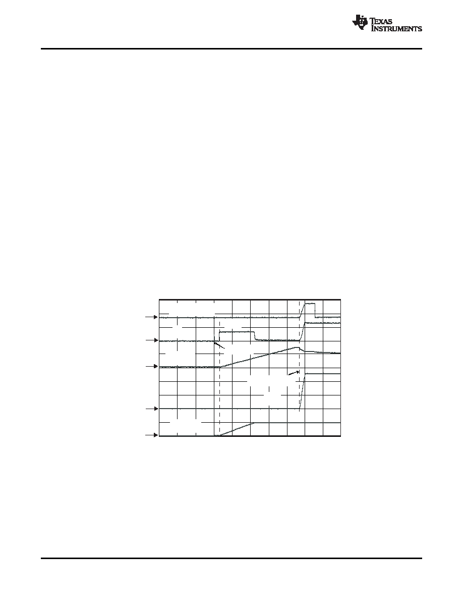
The internal PoE UVLO (Under Voltage Lock Out) circuit holds the hotswap switch off before the PSE provides
full voltage to the PD. This prevents the converter circuits from loading the PoE input during detection and
classification. The converter circuits will discharge CIN, CVC, and CVB while the PD is unpowered. Thus VVDD-VRTN
will be a small voltage just after full voltage is applied to the PD, as seen in Figure 23. The PSE drives the PI
voltage to the operating range once it has decided to power up the PD. When VVDD rises above the UVLO
turn-on threshold (VUVLO-R, ~35 V) with RTN high, the TPS23754 enables the hotswap MOSFET with a ~140 mA
(inrush) current limit as seen in Figure 25. Converter switching is disabled while CIN charges and VRTN falls from
VVDD to nearly VVSS, however the converter startup circuit is allowed to charge CVC (the bootstrap startup
capacitor). Converter switching is allowed if the PD is not in inrush, OTSD is not active, and the VC UVLO
permits it. Once the inrush current falls about 10% below the inrush current limit, the PD current limit switches to
the operational level (~970 mA). Continuing the startup sequence shown in Figure 25, VVC continues to rise until
the startup threshold (VCUV, ~15 V or ~9 V) is exceeded, turning the startup source off and enabling switching.
The VB regulator is always active, powering the internal converter circuits as VVC rises. There is a slight delay
between the removal of charge current and the start of switching as the softstart ramp sweeps above the VZDC
threshold. VVC falls as it powers both the internal circuits and the switching MOSFET gates. If the converter
control bias output rises to support VVC before it falls to VCUV – VCUVH (~8.5 V or ~5.5 V), a successful startup
occurs. T2P in Figure 23 (Figure 1, VT2P-OUT) becomes active within tT2P from the start of switching, indicating
that a type 2 PSE or an adapter is plugged in.
Figure 25. Power Up and Start
If VVDD- VVSS drops below the lower PoE UVLO (VUVLO-R - VUVLO-H, ~30.5 V), the hotswap MOSFET is turned off,
but the converter will still run. The converter will stop if VVC falls below the converter UVLO (VCUV – VCUVH, ~8.5 V
or ~5.5 V), the hotswap is in inrush current limit, 0% duty cycle is demanded by VCTL (VCTL < VZDC, ~1.5 V), or
the converter is in thermal shutdown.
20
Copyright 2008–2009, Texas Instruments Incorporated
相关PDF资料 |
PDF描述 |
|---|---|
| TPS23754PWP | 1.1 A SWITCHING CONTROLLER, 278 kHz SWITCHING FREQ-MAX, PDSO20 |
| TPS2375PWG4 | 1-CHANNEL POWER SUPPLY SUPPORT CKT, PDSO8 |
| TPS2376PWR | 1-CHANNEL POWER SUPPLY SUPPORT CKT, PDSO8 |
| TPS2375DRG4 | 1-CHANNEL POWER SUPPLY SUPPORT CKT, PDSO8 |
| TPS2375DG4 | 1-CHANNEL POWER SUPPLY SUPPORT CKT, PDSO8 |
相关代理商/技术参数 |
参数描述 |
|---|---|
| TPS23756PWPR | 功能描述:热插拔功率分布 Hi Pwr Eff PoE Inter face & DC/DC Cntrlr RoHS:否 制造商:Texas Instruments 产品:Controllers & Switches 电流限制: 电源电压-最大:7 V 电源电压-最小:- 0.3 V 工作温度范围: 功率耗散: 安装风格:SMD/SMT 封装 / 箱体:MSOP-8 封装:Tube |
| TPS23757EVM | 功能描述:电源管理IC开发工具 TPS23757 Eval Mod RoHS:否 制造商:Maxim Integrated 产品:Evaluation Kits 类型:Battery Management 工具用于评估:MAX17710GB 输入电压: 输出电压:1.8 V |
| TPS23757PW | 功能描述:热插拔功率分布 Hi Eff PoE Inter & DC/DC Controller RoHS:否 制造商:Texas Instruments 产品:Controllers & Switches 电流限制: 电源电压-最大:7 V 电源电压-最小:- 0.3 V 工作温度范围: 功率耗散: 安装风格:SMD/SMT 封装 / 箱体:MSOP-8 封装:Tube |
| TPS23757PWR | 功能描述:热插拔功率分布 Hi Eff PoE Interface & DC/DC Controller RoHS:否 制造商:Texas Instruments 产品:Controllers & Switches 电流限制: 电源电压-最大:7 V 电源电压-最小:- 0.3 V 工作温度范围: 功率耗散: 安装风格:SMD/SMT 封装 / 箱体:MSOP-8 封装:Tube |
| TPS2375D | 功能描述:热插拔功率分布 IEEE 802.3af PoE Pwr Device Cntrler RoHS:否 制造商:Texas Instruments 产品:Controllers & Switches 电流限制: 电源电压-最大:7 V 电源电压-最小:- 0.3 V 工作温度范围: 功率耗散: 安装风格:SMD/SMT 封装 / 箱体:MSOP-8 封装:Tube |
发布紧急采购,3分钟左右您将得到回复。