- 您现在的位置:买卖IC网 > PDF目录69503 > TPS23756PWP (TEXAS INSTRUMENTS INC) 1.1 A SWITCHING CONTROLLER, 278 kHz SWITCHING FREQ-MAX, PDSO20 PDF资料下载
参数资料
| 型号: | TPS23756PWP |
| 厂商: | TEXAS INSTRUMENTS INC |
| 元件分类: | 稳压器 |
| 英文描述: | 1.1 A SWITCHING CONTROLLER, 278 kHz SWITCHING FREQ-MAX, PDSO20 |
| 封装: | GREEN, PLASTIC, HTSSOP-20 |
| 文件页数: | 18/41页 |
| 文件大小: | 1405K |
| 代理商: | TPS23756PWP |
第1页第2页第3页第4页第5页第6页第7页第8页第9页第10页第11页第12页第13页第14页第15页第16页第17页当前第18页第19页第20页第21页第22页第23页第24页第25页第26页第27页第28页第29页第30页第31页第32页第33页第34页第35页第36页第37页第38页第39页第40页第41页
M1
R
C
S
C
O
U
T
2
D
VC1
GATE
R
T
N
,
C
O
M
A
R
T
N
V
C
CS
C
V
C
CTL
V
B
5
8
V
0
.1
u
F
R
D
E
N
F
ro
m
E
th
e
rn
e
t
P
a
ir
s
1
,2
V
SS
C
IN
R
C
T
L
C
T
L
F
ro
m
E
th
e
rn
e
t
P
a
ir
s
3
,4
CLS
DEN
FRS
T2P
R
C
L
S
R
T2P_OUT
R
F
R
S
V
B
C
V
B
R
F
B
U
R
F
B
L
TLV431
R
OB
C
IZ
V
OUT
PAD
V
D
GAT2
M2
R
T2P
D
A
R
A
P
D
2
R
APD1
PPD
A
d
a
p
te
r
D
T
R
B
L
N
K
APD
R
D
T
B
L
N
K
V
D
1
C
O
U
T
1
L
OUT
T1
T2
C
IO
V
T2P_OUT
TPS23754
TPS23754-1
TPS23756
www.ti.com
SLVS885D – OCTOBER 2008 – REVISED DECEMBER 2009
Several examples will demonstrate the limitations inherent in ORing solutions. Diode ORing a 48 V adapter with
PoE (option 1) presents the problem that either source might be higher. A blocking switch would be required to
assure which source was active. A second example is combining a 12 V adapter with PoE using option 2. The
converter will draw approximately four times the current at 12 V from the adapter than it does from PoE at 48 V.
Transition from adapter power to PoE may demand more current than can be supplied by the PSE. The
converter must be turned off while CIN capacitance charges, with a subsequent converter restart at the higher
voltage and lower input current. A third example is use of a 12 V adapter with ORing option 1. The PD hotswap
would have to handle four times the current, and have 1/16 the resistance (be 16 times larger) to dissipate equal
power. A fourth example is that MPS is lost when running from the adapter, causing the PSE to remove power
from the PD. If ac power is then lost, the PD will stop operating until the PSE detects and powers the PD.
APPLICATION INFORMATION
The TPS23754 will support many power supply topologies that require a single PWM gate drive or two
complementary gate drives and will operate with current-mode control. Figure 1 provides an example of an active
clamp forward converter that uses the second gate driver to control M2, the active element in the clamp. GAT2
may also be used to drive a synchronous rectifier as demonstrated in Figure 28. The TPS23754 may be used in
topologies that do not require GAT2, which may be disabled to reduce its idling loss.
Selecting a converter topology along with a design procedure is beyond the scope of this applications section.
Examples to help in programming the TPS23754 are shown below. Additional special topics are included to
explain the ORing capabilities, frequency dithering, and other design considerations.
For more specific converter design examples refer to the following application notes:
Designing with the TPS23753 Powered Device and Power Supply Controller, SLVA305
Designing for High Efficiency with the Active Clamp UCC2891 PWM Controller, SLUA303
Advanced Adapter ORing Solutions using the TPS23753, SLVA306A
TPS23754EVM-420 EVM: Evaluation Module for TPS23754, SLVU301
TPS23754EVM-383 EVM: Evaluation Module for TPS23754, SLVU304
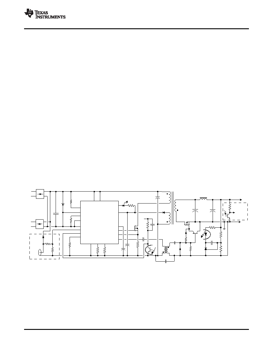
Figure 28. Driven Synchronous Flyback
Input Bridges and Schottky Diodes
Using Schottky diodes instead of PN junction diodes for the PoE input bridges and DVDD will reduce the loss of
this function by about 30%. There are however some things to consider when using them.
The IEEE standard specifies a maximum backfeed voltage of 2.8 V. A 100 k
resistor is placed between the
unpowered pairs and the voltage is measured across the resistor. Schottky diodes often have a higher reverse
leakage current than PN diodes, making this a harder requirement to meet. Use conservative design for diode
operating temperature, select lower-leakage devices where possible, and match leakage and temperatures by
using packaged bridges to help with this.
Copyright 2008–2009, Texas Instruments Incorporated
25
相关PDF资料 |
PDF描述 |
|---|---|
| TPS23754PWP | 1.1 A SWITCHING CONTROLLER, 278 kHz SWITCHING FREQ-MAX, PDSO20 |
| TPS2375PWG4 | 1-CHANNEL POWER SUPPLY SUPPORT CKT, PDSO8 |
| TPS2376PWR | 1-CHANNEL POWER SUPPLY SUPPORT CKT, PDSO8 |
| TPS2375DRG4 | 1-CHANNEL POWER SUPPLY SUPPORT CKT, PDSO8 |
| TPS2375DG4 | 1-CHANNEL POWER SUPPLY SUPPORT CKT, PDSO8 |
相关代理商/技术参数 |
参数描述 |
|---|---|
| TPS23756PWPR | 功能描述:热插拔功率分布 Hi Pwr Eff PoE Inter face & DC/DC Cntrlr RoHS:否 制造商:Texas Instruments 产品:Controllers & Switches 电流限制: 电源电压-最大:7 V 电源电压-最小:- 0.3 V 工作温度范围: 功率耗散: 安装风格:SMD/SMT 封装 / 箱体:MSOP-8 封装:Tube |
| TPS23757EVM | 功能描述:电源管理IC开发工具 TPS23757 Eval Mod RoHS:否 制造商:Maxim Integrated 产品:Evaluation Kits 类型:Battery Management 工具用于评估:MAX17710GB 输入电压: 输出电压:1.8 V |
| TPS23757PW | 功能描述:热插拔功率分布 Hi Eff PoE Inter & DC/DC Controller RoHS:否 制造商:Texas Instruments 产品:Controllers & Switches 电流限制: 电源电压-最大:7 V 电源电压-最小:- 0.3 V 工作温度范围: 功率耗散: 安装风格:SMD/SMT 封装 / 箱体:MSOP-8 封装:Tube |
| TPS23757PWR | 功能描述:热插拔功率分布 Hi Eff PoE Interface & DC/DC Controller RoHS:否 制造商:Texas Instruments 产品:Controllers & Switches 电流限制: 电源电压-最大:7 V 电源电压-最小:- 0.3 V 工作温度范围: 功率耗散: 安装风格:SMD/SMT 封装 / 箱体:MSOP-8 封装:Tube |
| TPS2375D | 功能描述:热插拔功率分布 IEEE 802.3af PoE Pwr Device Cntrler RoHS:否 制造商:Texas Instruments 产品:Controllers & Switches 电流限制: 电源电压-最大:7 V 电源电压-最小:- 0.3 V 工作温度范围: 功率耗散: 安装风格:SMD/SMT 封装 / 箱体:MSOP-8 封装:Tube |
发布紧急采购,3分钟左右您将得到回复。