- 您现在的位置:买卖IC网 > PDF目录69503 > TPS23756PWP (TEXAS INSTRUMENTS INC) 1.1 A SWITCHING CONTROLLER, 278 kHz SWITCHING FREQ-MAX, PDSO20 PDF资料下载
参数资料
| 型号: | TPS23756PWP |
| 厂商: | TEXAS INSTRUMENTS INC |
| 元件分类: | 稳压器 |
| 英文描述: | 1.1 A SWITCHING CONTROLLER, 278 kHz SWITCHING FREQ-MAX, PDSO20 |
| 封装: | GREEN, PLASTIC, HTSSOP-20 |
| 文件页数: | 27/41页 |
| 文件大小: | 1405K |
| 代理商: | TPS23756PWP |
第1页第2页第3页第4页第5页第6页第7页第8页第9页第10页第11页第12页第13页第14页第15页第16页第17页第18页第19页第20页第21页第22页第23页第24页第25页第26页当前第27页第28页第29页第30页第31页第32页第33页第34页第35页第36页第37页第38页第39页第40页第41页
+
-
4
9
.9
kW
1
0
kW
4
.9
9
kW
6.04kW
10kW
0
.0
1m
F
301kW
1 F
m
V
B
To
FRS
ARTN
TL331IDBV
TPS23754
TPS23754-1
TPS23756
www.ti.com
SLVS885D – OCTOBER 2008 – REVISED DECEMBER 2009
Special Switching MOSFET Considerations
Special care must be used in selecting the converter switching MOSFET. The TPS23756 minimum switching
MOSFET VGATE is ~5.5 V, which is due to the VC lower threshold. This will occur during an output overload, or
towards the end of a (failed) bootstrap startup. The MOSFET must be able to carry the anticipated peak fault
current at this gate voltage.
Thermal Considerations and OTSD
Sources of nearby local PCB heating should be considered during the thermal design. Typical calculations
assume that the TPS23754 is the only heat source contributing to the PCB temperature rise. It is possible for a
normally operating TPS23754 device to experience an OTSD event if it is excessively heated by a nearby
device.
Frequency Dithering for Conducted Emissions Control
The international standard CISPR 22 (and adopted versions) is often used as a requirement for conducted
emissions. Ethernet cables are covered as a telecommunication port under section 5.2 for conducted emissions.
Meeting EMI requirements is often a challenge, with the lower limits of Class B being especially hard. Circuit
board layout, filtering, and snubbing various nodes in the power circuit are the first layer of control techniques. A
more detailed discussion of EMI control is presented in Practical Guidelines to Designing an EMI Compliant PoE
Powered Device With Isolated Flyback, TI literature number SLUA469. Additionally, IEEE802.3at sections 33.3
and 33.4 have requirements for noise injected onto the Ethernet cable based on compatibility with data
transmission.
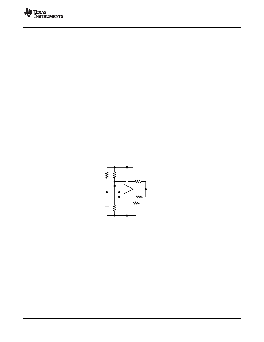
Occasionally, a technique referred to as frequency dithering is utilized to provide additional EMI measurement
reduction. The switching frequency is modulated to spread the narrowband individual harmonics across a wider
bandwidth, thus lowering peak measurements. The circuit of Figure 37 modulates the switching frequency by
feeding a small ac signal into the FRS pin. These values may be adapted to suit individual needs.
Figure 37. Frequency Dithering
ESD
The TPS23754 has been tested to EN61000-4-2 using a power supply based on Figure 1. The levels used were
8 kV contact discharge and 15 kV air discharge. Surges were applied between the PoE input and the dc output,
between the adapter input and the dc output, between the adapter and the PoE inputs, and to the dc output with
respect to earth. Tests were done both powered and unpowered. No TPS23754 failures were observed and
operation was continuous. See Figure 29 for additional protection for some test configurations.
ESD requirements for a unit that incorporates the TPS23754 have a much broader scope and operational
implications than are used in TI’s testing. Unit-level requirements should not be confused with reference design
testing that only validates the ruggedness of the TPS23754.
Layout
Printed circuit board layout recommendations are provided in the evaluation module (EVM) documentation
available for these devices.
Copyright 2008–2009, Texas Instruments Incorporated
33
相关PDF资料 |
PDF描述 |
|---|---|
| TPS23754PWP | 1.1 A SWITCHING CONTROLLER, 278 kHz SWITCHING FREQ-MAX, PDSO20 |
| TPS2375PWG4 | 1-CHANNEL POWER SUPPLY SUPPORT CKT, PDSO8 |
| TPS2376PWR | 1-CHANNEL POWER SUPPLY SUPPORT CKT, PDSO8 |
| TPS2375DRG4 | 1-CHANNEL POWER SUPPLY SUPPORT CKT, PDSO8 |
| TPS2375DG4 | 1-CHANNEL POWER SUPPLY SUPPORT CKT, PDSO8 |
相关代理商/技术参数 |
参数描述 |
|---|---|
| TPS23756PWPR | 功能描述:热插拔功率分布 Hi Pwr Eff PoE Inter face & DC/DC Cntrlr RoHS:否 制造商:Texas Instruments 产品:Controllers & Switches 电流限制: 电源电压-最大:7 V 电源电压-最小:- 0.3 V 工作温度范围: 功率耗散: 安装风格:SMD/SMT 封装 / 箱体:MSOP-8 封装:Tube |
| TPS23757EVM | 功能描述:电源管理IC开发工具 TPS23757 Eval Mod RoHS:否 制造商:Maxim Integrated 产品:Evaluation Kits 类型:Battery Management 工具用于评估:MAX17710GB 输入电压: 输出电压:1.8 V |
| TPS23757PW | 功能描述:热插拔功率分布 Hi Eff PoE Inter & DC/DC Controller RoHS:否 制造商:Texas Instruments 产品:Controllers & Switches 电流限制: 电源电压-最大:7 V 电源电压-最小:- 0.3 V 工作温度范围: 功率耗散: 安装风格:SMD/SMT 封装 / 箱体:MSOP-8 封装:Tube |
| TPS23757PWR | 功能描述:热插拔功率分布 Hi Eff PoE Interface & DC/DC Controller RoHS:否 制造商:Texas Instruments 产品:Controllers & Switches 电流限制: 电源电压-最大:7 V 电源电压-最小:- 0.3 V 工作温度范围: 功率耗散: 安装风格:SMD/SMT 封装 / 箱体:MSOP-8 封装:Tube |
| TPS2375D | 功能描述:热插拔功率分布 IEEE 802.3af PoE Pwr Device Cntrler RoHS:否 制造商:Texas Instruments 产品:Controllers & Switches 电流限制: 电源电压-最大:7 V 电源电压-最小:- 0.3 V 工作温度范围: 功率耗散: 安装风格:SMD/SMT 封装 / 箱体:MSOP-8 封装:Tube |
发布紧急采购,3分钟左右您将得到回复。