- 您现在的位置:买卖IC网 > PDF目录202172 > V58C2256404SBJ5 (PROMOS TECHNOLOGIES INC) 64M X 4 DDR DRAM, 0.65 ns, PBGA60 PDF资料下载
参数资料
| 型号: | V58C2256404SBJ5 |
| 厂商: | PROMOS TECHNOLOGIES INC |
| 元件分类: | DRAM |
| 英文描述: | 64M X 4 DDR DRAM, 0.65 ns, PBGA60 |
| 封装: | LEAD FREE, MO-233, FBGA-60 |
| 文件页数: | 62/62页 |
| 文件大小: | 983K |
| 代理商: | V58C2256404SBJ5 |
第1页第2页第3页第4页第5页第6页第7页第8页第9页第10页第11页第12页第13页第14页第15页第16页第17页第18页第19页第20页第21页第22页第23页第24页第25页第26页第27页第28页第29页第30页第31页第32页第33页第34页第35页第36页第37页第38页第39页第40页第41页第42页第43页第44页第45页第46页第47页第48页第49页第50页第51页第52页第53页第54页第55页第56页第57页第58页第59页第60页第61页当前第62页
9
ProMOS TECHNOLOGIES
V58C2256(804/404/164)SB
V58C2256(804/404/164)SB Rev. 1.0 November 2003
Functional Description
■ Power-Up Sequence
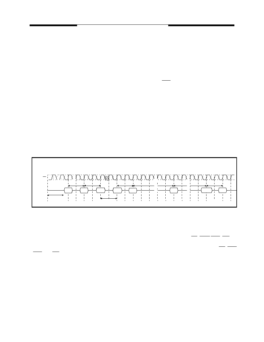
The following sequence is required for POWER UP.
1. Apply power and attempt to maintain CKE at a low state (all other inputs may be undefined.)
- Apply VDD before or at the same time as VDDQ.
- Apply VDDQ before or at the same time as VTT & Vref.
2. Start clock and maintain stable condition for a minimum of 200us.
3. The minimum of 200us after stable power and clock (CLK, CLK), apply NOP & take CKE high.
4. Precharge all banks.
5. Issue EMRS to enable DLL.(To issue “DLL Enable” command, provide “Low” to A0, “High” to BA0
and “Low” to all of the rest address pins, A1~A12 and BA1)
6. Issue a mode register set command for “DLL reset”. The additional 200 cycles of clock input is
required to lock the DLL. (To issue DLL reset command, provide “High” to A8 and “Low” to BA0)
7. Issue precharge commands for all banks of the device.
8. Issue 2 or more auto-refresh commands.
9. Issue a mode register set command to initialize device operation.
Note1 Every “DLL enable” command resets DLL. Therefore sequence 6 can be skipped during power up. Instead of it,
the additional 200 cycles of clock input is required to lock the DLL after enabling DLL.
Extended Mode Register Set (EMRS)
The extended mode register stores the data for enabling or disabling DLL. The default value of the extend-
ed mode register is not defined, therefore the extended mode register must be written after power up for en-
abling or disabling DLL. The extended mode register is written by asserting low on CS, RAS, CAS, WE and
high on BA0 (The DDR SDRAM should be in all bank precharge with CKE already high prior to writing into
the extended mode register). The state of address pins A0 ~ A12 and BA1 in the same cycle as CS, RAS,
CAS and WE low is written in the extended mode register. Two clock cycles are required to complete the
write operation in the extended mode register. The mode register contents can be changed using the same
command and clock cycle requirements during operation as long as all banks are in the idle state. A0 is used
for DLL enable or disable. “High” on BA0 is used for EMRS. All the other address pins except A0 and BA0
must be set to low for proper EMRS operation. A
1 is used at EMRS to indicate I/O strength A1 = 0 full strength,
A
1 = 1 half strength. Refer to the table for specific codes.
Power up Sequence & Auto Refresh(CBR)
Command
0
1
2
3
4
5
6
7
8
9
10
11
12
13
14
15
16
17
18
19
tRP
2 Clock min.
precharge
ALL Banks
2nd Auto
Refresh
Mode
Register Set
Any
Command
tRFC
1st Auto
Refresh
tRFC
min. 200 Cycle
CK, CK
EMRS
MRS
2 Clock min.
200
S Power up
to 1st command
DLL Reset
2 Clock min.
6
5
47
8
precharge
ALL Banks
相关PDF资料 |
PDF描述 |
|---|---|
| V58C2256164SBLJ5B | 16M X 16 DDR DRAM, 0.65 ns, PBGA60 |
| V58C2256404SCLS7I | 64M X 4 DDR DRAM, 0.75 ns, PBGA60 |
| V58C2256404SHUT6E | 64M X 4 DDR DRAM, PDSO66 |
| V58C2256804SHLJ5E | 32M X 8 DDR DRAM, PBGA60 |
| V58C2256804SHUE6E | 32M X 8 DDR DRAM, PDSO66 |
相关代理商/技术参数 |
参数描述 |
|---|---|
| V58C2256804S | 制造商:MOSEL 制造商全称:MOSEL 功能描述:HIGH PERFORMANCE 2.5 VOLT 256 Mbit DDR SDRAM |
| V58C2256804SAT-5 | 制造商:Mosel Vitelic Corporation 功能描述:SDRAM, DDR, 32M x 8, 66 Pin, Plastic, TSSOP |
| V58C265164S | 制造商:MOSEL 制造商全称:MOSEL 功能描述:64 Mbit DDR SDRAM 2.5 VOLT 4M X 16 |
| V58C265404S | 制造商:MOSEL 制造商全称:MOSEL 功能描述:HIGH PERFORMANCE 2.5 VOLT 16M X 4 DDR SDRAM 4 BANKS X 4Mbit X 4 |
| V58C265804S | 制造商:MOSEL 制造商全称:MOSEL 功能描述:HIGH PERFORMANCE 2.5 VOLT 8M X 8 DDR SDRAM 4 BANKS X 2Mbit X 8 |
发布紧急采购,3分钟左右您将得到回复。