参数资料
| 型号: | W25Q16BVZPIG |
| 厂商: | Winbond Electronics |
| 文件页数: | 23/68页 |
| 文件大小: | 0K |
| 描述: | IC SPI FLASH 16MBIT 8WSON |
| 标准包装: | 100 |
| 系列: | SpiFlash® |
| 格式 - 存储器: | 闪存 |
| 存储器类型: | FLASH |
| 存储容量: | 16M(2M x 8) |
| 速度: | 104MHz |
| 接口: | SPI 串行 |
| 电源电压: | 2.7 V ~ 3.6 V |
| 工作温度: | -40°C ~ 85°C |
| 封装/外壳: | 8-WDFN 裸露焊盘 |
| 供应商设备封装: | 8-WSON(6x5) |
| 包装: | 管件 |
第1页第2页第3页第4页第5页第6页第7页第8页第9页第10页第11页第12页第13页第14页第15页第16页第17页第18页第19页第20页第21页第22页当前第23页第24页第25页第26页第27页第28页第29页第30页第31页第32页第33页第34页第35页第36页第37页第38页第39页第40页第41页第42页第43页第44页第45页第46页第47页第48页第49页第50页第51页第52页第53页第54页第55页第56页第57页第58页第59页第60页第61页第62页第63页第64页第65页第66页第67页第68页
�� �
�
�W25Q16BV�
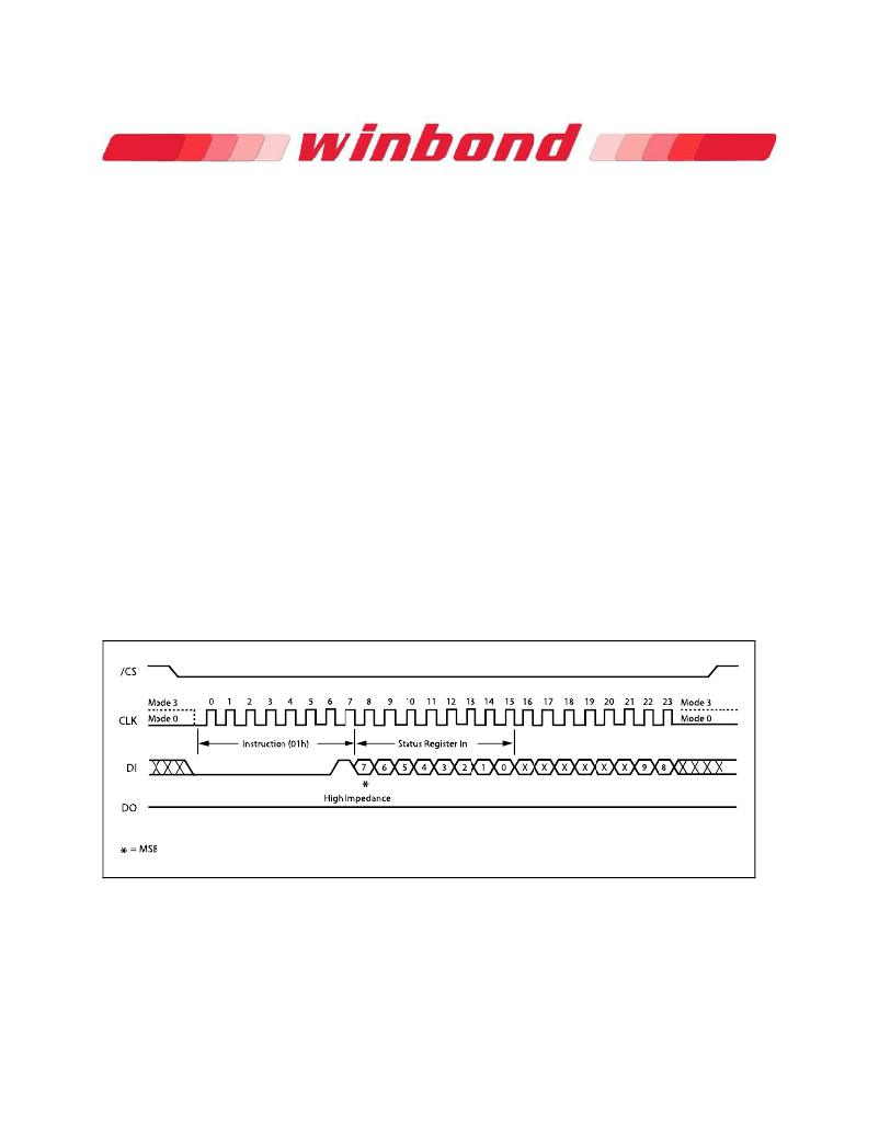
�11.2.8� Write� Status� Register� (01h)�
�The� Write� Status� Register� instruction� allows� the� Status� Register� to� be� written.� A� Write� Enable� instruction�
�must� previously� have� been� executed� for� the� device� to� accept� the� Write� Status� Register� Instruction� (Status�
�Register� bit� WEL� must� equal� 1).� Once� write� enabled,� the� instruction� is� entered� by� driving� /CS� low,�
�sending� the� instruction� code� “01h”,� and� then� writing� the� status� register� data� byte� as� illustrated� in� figure� 7.�
�The� Status� Register� bits� are� shown� in� figure� 3� and� described� earlier� in� this� datasheet.�
�Only� non-volatile� Status� Register� bits� SRP0,� SEC,� TB,� BP2,� BP1,� BP0� (bits� 7,� 5,� 4,� 3,� 2� of� Status�
�Register-1)� and� QE,� SRP1(bits� 9� and� 8� of� Status� Register-2)� can� be� written� to.� All� other� Status� Register�
�bit� locations� are� read-only� and� will� not� be� affected� by� the� Write� Status� Register� instruction.�
�The� /CS� pin� must� be� driven� high� after� the� eighth� or� sixteenth� bit� of� data� that� is� clocked� in.� If� this� is� not�
�done� the� Write� Status� Register� instruction� will� not� be� executed.� If� /CS� is� driven� high� after� the� eighth� clock�
�(compatible� with� the� 25X� series)� the� QE� and� SRP1� bits� will� be� cleared� to� 0.� After� /CS� is� driven� high,� the�
�self-timed� Write� Status� Register� cycle� will� commence� for� a� time� duration� of� t� W� (See� AC� Characteristics).�
�While� the� Write� Status� Register� cycle� is� in� progress,� the� Read� Status� Register� instruction� may� still� be�
�accessed� to� check� the� status� of� the� BUSY� bit.� The� BUSY� bit� is� a� 1� during� the� Write� Status� Register� cycle�
�and� a� 0� when� the� cycle� is� finished� and� ready� to� accept� other� instructions� again.� After� the� Write� Register�
�cycle� has� finished� the� Write� Enable� Latch� (WEL)� bit� in� the� Status� Register� will� be� cleared� to� 0.�
�The� Write� Status� Register� instruction� allows� the� Block� Protect� bits� (SEC,� TB,� BP2,� BP1� and� BP0)� to� be�
�set� for� protecting� all,� a� portion,� or� none� of� the� memory� from� erase� and� program� instructions.� Protected�
�areas� become� read-only� (see� Status� Register� Memory� Protection� table� and� description).� The� Write� Status�
�Register� instruction� also� allows� the� Status� Register� Protect� bits� (SRP0,� SRP1)� to� be� set.� Those� bits� are�
�used� in� conjunction� with� the� Write� Protect� (/WP)� pin,� Lock� out� or� OTP� features� to� disable� writes� to� the�
�status� register.� Please� refer� to� 11.1.6� for� detailed� descriptions� regarding� Status� Register� protection�
�methods.� Factory� default� for� all� status� Register� bits� are� 0.�
�Figure� 7.� Write� Status� Register� Instruction� Sequence� Diagram�
�Publication� Release� Date:� July� 08,� 2010�
�-� 23� -�
�Revision� F�
�相关PDF资料 |
PDF描述 |
|---|---|
| W25Q80BVDAIG | SPI FLASH 8MBIT 8-DIP |
| EP1S10F780C6N | IC STRATIX FPGA 10K LE 780-FBGA |
| EPF10K30AFC484-1 | IC FLEX 10KA FPGA 30K 484-FBGA |
| W25X20CLZPIG | IC FLASH SPI 2MBIT 8WSON |
| AX1000-FGG484I | IC FPGA AXCELERATOR 1M 484-FBGA |
相关代理商/技术参数 |
参数描述 |
|---|---|
| W25Q16BVZPIP | 制造商:WINBOND 制造商全称:Winbond 功能描述:16M-BIT SERIAL FLASH MEMORY WITH DUAL AND QUAD SPI |
| W25Q16CL | 制造商:WINBOND 制造商全称:Winbond 功能描述:2.5V 16M-BIT SERIAL FLASH MEMORY WITH DUAL AND QUAD SPI |
| W25Q16CLDAIG | 制造商:WINBOND 制造商全称:Winbond 功能描述:2.5V 16M-BIT SERIAL FLASH MEMORY WITH DUAL AND QUAD SPI |
| W25Q16CLDAIP | 制造商:WINBOND 制造商全称:Winbond 功能描述:2.5V 16M-BIT SERIAL FLASH MEMORY WITH DUAL AND QUAD SPI |
| W25Q16CLSFIG | 制造商:WINBOND 制造商全称:Winbond 功能描述:2.5V 16M-BIT SERIAL FLASH MEMORY WITH DUAL AND QUAD SPI |
发布紧急采购,3分钟左右您将得到回复。