- 您现在的位置:买卖IC网 > PDF目录203637 > W947D6HBHX6E (WINBOND ELECTRONICS CORP) 8M X 16 DDR DRAM, 5 ns, PBGA60 PDF资料下载
参数资料
| 型号: | W947D6HBHX6E |
| 厂商: | WINBOND ELECTRONICS CORP |
| 元件分类: | DRAM |
| 英文描述: | 8M X 16 DDR DRAM, 5 ns, PBGA60 |
| 封装: | 8 X 9 MM, 0.80 MM PITCH, HALOGEN FREE AND LEAD FREE, VFBGA-60 |
| 文件页数: | 49/60页 |
| 文件大小: | 1160K |
| 代理商: | W947D6HBHX6E |
第1页第2页第3页第4页第5页第6页第7页第8页第9页第10页第11页第12页第13页第14页第15页第16页第17页第18页第19页第20页第21页第22页第23页第24页第25页第26页第27页第28页第29页第30页第31页第32页第33页第34页第35页第36页第37页第38页第39页第40页第41页第42页第43页第44页第45页第46页第47页第48页当前第49页第50页第51页第52页第53页第54页第55页第56页第57页第58页第59页第60页
W947D6HB / W947D2HB
128Mb Mobile LPDDR
Publication Release Date:Jun,17, 2011
- 53 -
Revision A01-003
Notes:
1.
All voltages referenced to VSS.
2.
All parameters assume proper device initialization.
3.
Tests for AC timing may be conducted at nominal supply voltage levels, but the related specifications and
device operation are guaranteed for the full voltage and temperature range specified.
4.
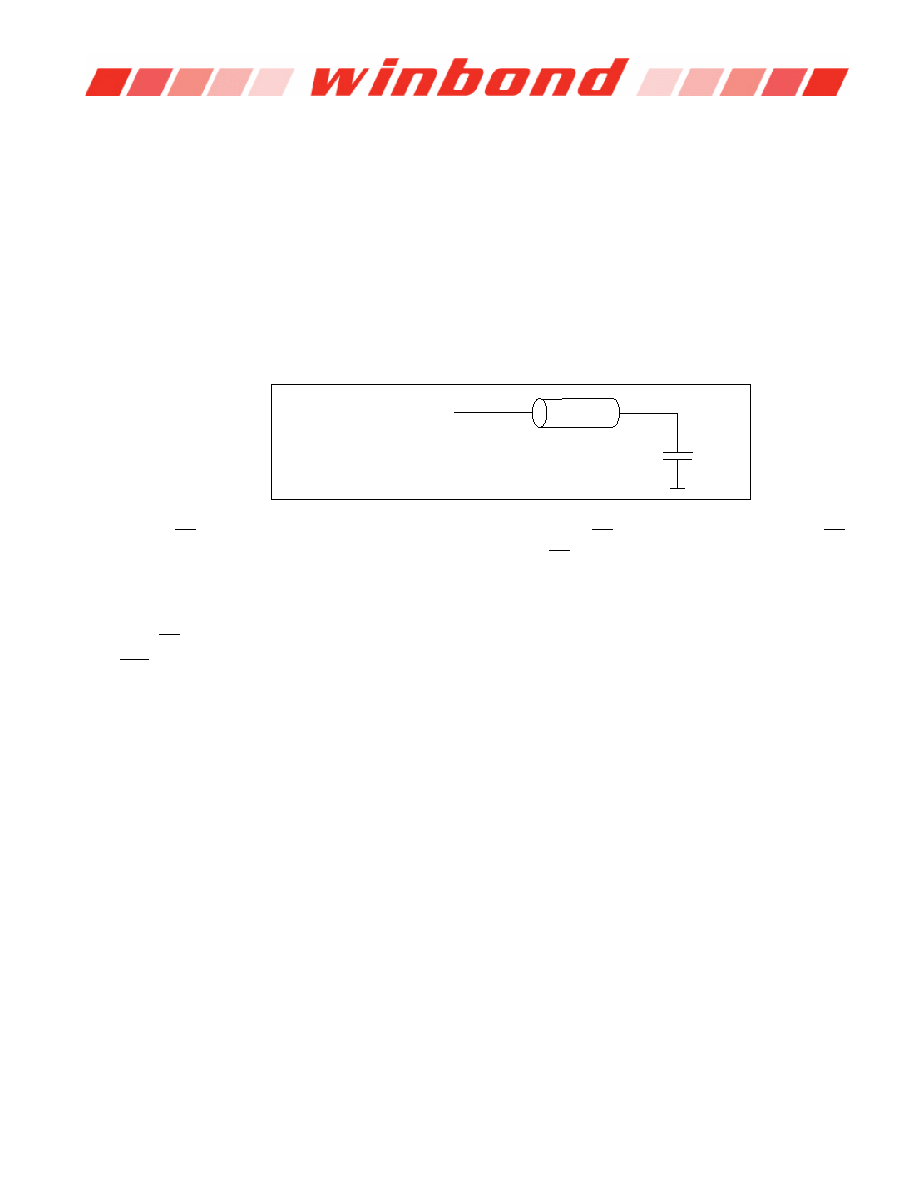
The circuit shown below represents the timing reference load used in defining the relevant timing parameters
of the part. It is not intended to be either a precise representation of the typical system environment nor a
depiction of the actual load presented by a production tester. System designers will use IBIS or other
simulation tools to correlate the timing reference load to system environment. Manufacturers will correlate to
their production test conditions (generally a coaxial transmission line terminated at the tester electronics). For
the half strength driver with a nominal 10pF load parameters tAC and tQH are expected to be in the same
range. However, these parameters are not subject to production test but are estimated by design /
characterization. Use of IBIS or other simulation tools for system design validation is suggested.
Time Reference Load
I/O
Z0 = 50 Ohms
20pF
5.
The CK/ CK input reference voltage level (for timing referenced to CK/ CK ) is the point at which CK and CK
cross; the input reference voltage level for signals other than CK/ CK is VDDQ/2.
6.
The timing reference voltage level is VDDQ/2.
7.
AC and DC input and output voltage levels are defined in the section for Electrical Characteristics and AC/DC
operating conditions.
8.
A CK/ CK differential slew rate of 2.0 V/ns is assumed for all parameters.
9.
CAS latency definition: with CL = 3 the first data element is valid at (2 * tCK + tAC) after the clock at which
the READ command was registered; with CL = 2 the first data element is valid at (tCK + tAC) after the clock at
which the READ command was registered
10. Min (tCL, tCH) refers to the smaller of the actual clock low time and the actual clock high time as provided to
the device (i.e. this value can be greater than the minimum specification limits of tCL and tCH)
11. tQH = tHP - tQHS, where tHP = minimum half clock period for any given cycle and is defined by clock high or
clock low (tCL, tCH). tQHS accounts for 1) the pulse duration distortion of on-chip clock circuits; and 2) the
worst case push-out of DQS on one transition followed by the worst case pull-in of DQ on the next transition,
both of which are, separately, due to data pin skew and output pattern effects, and p-channel to n-channel
variation of the output drivers.
12. The only time that the clock frequency is allowed to change is during clock stop, power-down or self-refresh
modes.
13. The transition time for DQ, DM and DQS inputs is measured between VIL(DC) to VIH(AC) for rising input
signals, and VIH(DC) to VIL(AC) for falling input signals.
14. DQS, DM and DQ input slew rate is specified to prevent double clocking of data and preserve setup and hold
times. Signal transitions through the DC region must be monotonic.
15. Input sle
w rate ≥ 1.0 V/ns.
16.
Input slew rate ≥ 0.5 V/ns and < 1.0 V/ns.
17. These parameters guarantee device timing but they are not necessarily tested on each device.
18. The transition time for address and command inputs is measured between VIH and VIL.
相关PDF资料 |
PDF描述 |
|---|---|
| W9602BB | PUSHBUTTON SWITCH, SPST, MOMENTARY, 10A, 28VDC, PANEL MOUNT-THREADED |
| W9605BB | PUSHBUTTON SWITCH, SPST, MOMENTARY, 10A, 28VDC, PANEL MOUNT-THREADED |
| W9606BB | PUSHBUTTON SWITCH, SPDT, MOMENTARY, 10A, 28VDC, PANEL MOUNT-THREADED |
| W9712G8JB-3 | DDR DRAM, PBGA60 |
| W971GG6IB-25 | 32M X 16 DDR DRAM, 0.4 ns, PBGA84 |
相关代理商/技术参数 |
参数描述 |
|---|---|
| W947D6HBHX6G | 制造商:WINBOND 制造商全称:Winbond 功能描述:128Mb Mobile LPDDR |
| W948D2FB | 制造商:WINBOND 制造商全称:Winbond 功能描述:256Mb Mobile LPDDR |
| W948D2FBJX5E | 功能描述:IC LPDDR SDRAM 256MBIT 90VFBGA RoHS:是 类别:集成电路 (IC) >> 存储器 系列:- 标准包装:1 系列:- 格式 - 存储器:闪存 存储器类型:闪存 - NAND 存储容量:4G(256M x 16) 速度:- 接口:并联 电源电压:2.7 V ~ 3.6 V 工作温度:0°C ~ 70°C 封装/外壳:48-TFSOP(0.724",18.40mm 宽) 供应商设备封装:48-TSOP I 包装:Digi-Reel® 其它名称:557-1461-6 |
| W948D2FBJX5ETR | 制造商:Winbond Electronics Corp 功能描述:256M MDDR, X32, 200MHZ |
| W948D2FBJX5I | 制造商:Winbond Electronics Corp 功能描述:DRAM Chip DDR SDRAM 256M-Bit 8Mx32 1.8V 90-Pin VFBGA 制造商:Winbond Electronics Corp 功能描述:IC MEMORY |
发布紧急采购,3分钟左右您将得到回复。