参数资料
| 型号: | XA3SD1800A-4CSG484Q |
| 厂商: | Xilinx Inc |
| 文件页数: | 16/58页 |
| 文件大小: | 0K |
| 描述: | SPARTAN-3ADSP FPGA 1800K 484CSBG |
| 产品培训模块: | Extended Spartan 3A FPGA Family |
| 标准包装: | 84 |
| 系列: | Spartan®-3A DSP XA |
| LAB/CLB数: | 4160 |
| 逻辑元件/单元数: | 37440 |
| RAM 位总计: | 1548288 |
| 输入/输出数: | 309 |
| 门数: | 1800000 |
| 电源电压: | 1.14 V ~ 1.26 V |
| 安装类型: | 表面贴装 |
| 工作温度: | -40°C ~ 125°C |
| 封装/外壳: | 484-FBGA,CSPBGA |
| 供应商设备封装: | 484-CSPBGA |
| 配用: | 122-1574-ND - KIT DEVELOPMENT SPARTAN 3ADSP |
第1页第2页第3页第4页第5页第6页第7页第8页第9页第10页第11页第12页第13页第14页第15页当前第16页第17页第18页第19页第20页第21页第22页第23页第24页第25页第26页第27页第28页第29页第30页第31页第32页第33页第34页第35页第36页第37页第38页第39页第40页第41页第42页第43页第44页第45页第46页第47页第48页第49页第50页第51页第52页第53页第54页第55页第56页第57页第58页
XA Spartan-3A DSP Automotive FPGA Family Data Sheet
DS705 (v2.0) April 18, 2011
Product Specification
23
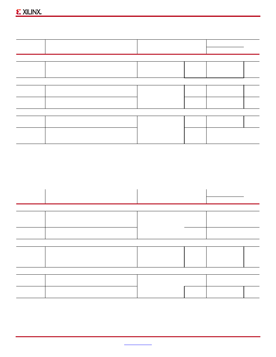
Output Propagation Times
Three-State Output Propagation Times
Table 24: Timing for the IOB Output Path
Symbol
Description
Conditions
Device
Speed Grade: -4
Units
Max
Clock-to-Output Times
TIOCKP
When reading from the Output Flip-Flop (OFF),
the time from the active transition at the OCLK
input to data appearing at the Output pin
LVCMOS25(2), 12 mA
output drive, Fast slew
rate
All
3.13
ns
Propagation Times
TIOOP
The time it takes for data to travel from the JOB’s
O input to the Output pin
LVCMOS25(2), 12 mA
output drive, Fast slew
rate
All
2.91
ns
TIOOLP
The time it takes for data to travel from the O input
through the OFF latch to the Output pin
All
2.85
ns
Set/Reset Times
TIOSRP
Time from asserting the OFF’s SR input to
setting/resetting data at the Output pin
LVCMOS25(2), 12 mA
output drive, Fast slew
rate
All
3.89
ns
TIOGSRQ
Time from asserting the Global Set Reset (GSR)
input on the STARTUP_SPARTAN3A primitive to
setting/resetting data at the Output pin
All
9.65
ns
Notes:
1.
The numbers in this table are tested using the methodology presented in Table 27 and are based on the operating conditions set forth in
2.
This time requires adjustment whenever a signal standard other than LVCMOS25 with 12 mA drive and Fast slew rate is assigned to the data
Output. When this is true, add the appropriate Output adjustment from Table 26.
Table 25: Timing for the IOB Three-State Path
Symbol
Description
Conditions
Device
Speed Grade: -4
Units
Max
Synchronous Output Enable/Disable Times
TIOCKHZ
Time from the active transition at the OTCLK input
of the Three-state Flip-Flop (TFF) to when the
Output pin enters the high-impedance state
LVCMOS25, 12 mA
output drive, Fast slew
rate
All
1.39
ns
TIOCKON(2)
Time from the active transition at TFF’s OTCLK
input to when the Output pin drives valid data
All
3.35
ns
Asynchronous Output Enable/Disable Times
TGTS
Time from asserting the Global Three State (GTS)
input on the STARTUP_SPARTAN3A primitive to
when the Output pin enters the high-impedance
state
LVCMOS25, 12 mA
output drive, Fast slew
rate
All
10.36
ns
Set/Reset Times
TIOSRHZ
Time from asserting TFF’s SR input to when the
Output pin enters a high-impedance state
LVCMOS25, 12 mA
output drive, Fast slew
rate
All
1.86
ns
TIOSRON(2)
Time from asserting TFF’s SR input at TFF to
when the Output pin drives valid data
All
3.82
ns
Notes:
1.
The numbers in this table are tested using the methodology presented in Table 27 and are based on the operating conditions set forth in
2.
This time requires adjustment whenever a signal standard other than LVCMOS25 with 12 mA drive and Fast slew rate is assigned to the data
Output. When this is true, add the appropriate Output adjustment from Table 26.
相关PDF资料 |
PDF描述 |
|---|---|
| XC6SLX100T-N3FGG484I | IC FPGA SPARTAN-6 484FPGA |
| 1-553035-8 | CONN CHAMP SHIELD RCPT 24POS |
| 828347-1 | CONN D-SUB FEM SCREW LOCK KIT |
| XC6SLX100T-N3CSG484I | IC FPGA SPARTAN-6 484CSBGA |
| XC6SLX100T-2FG484I | IC FPGA SPARTAN 6 484FGGBGA |
相关代理商/技术参数 |
参数描述 |
|---|---|
| XA3SD1800A-4FGG676I | 功能描述:SPARTAN-3ADSP FPGA 1800K 676FBGA RoHS:是 类别:集成电路 (IC) >> 嵌入式 - FPGA(现场可编程门阵列) 系列:Spartan®-3A DSP XA 产品变化通告:Step Intro and Pkg Change 11/March/2008 标准包装:1 系列:Virtex®-5 SXT LAB/CLB数:4080 逻辑元件/单元数:52224 RAM 位总计:4866048 输入/输出数:480 门数:- 电源电压:0.95 V ~ 1.05 V 安装类型:表面贴装 工作温度:-40°C ~ 100°C 封装/外壳:1136-BBGA,FCBGA 供应商设备封装:1136-FCBGA 配用:568-5088-ND - BOARD DEMO DAC1408D750122-1796-ND - EVALUATION PLATFORM VIRTEX-5 |
| XA3SD1800A-4FGG676Q | 功能描述:SPARTAN-3ADSP FPGA 1800K 676FBGA RoHS:是 类别:集成电路 (IC) >> 嵌入式 - FPGA(现场可编程门阵列) 系列:Spartan®-3A DSP XA 产品变化通告:Step Intro and Pkg Change 11/March/2008 标准包装:1 系列:Virtex®-5 SXT LAB/CLB数:4080 逻辑元件/单元数:52224 RAM 位总计:4866048 输入/输出数:480 门数:- 电源电压:0.95 V ~ 1.05 V 安装类型:表面贴装 工作温度:-40°C ~ 100°C 封装/外壳:1136-BBGA,FCBGA 供应商设备封装:1136-FCBGA 配用:568-5088-ND - BOARD DEMO DAC1408D750122-1796-ND - EVALUATION PLATFORM VIRTEX-5 |
| XA3SD3400A | 制造商:XILINX 制造商全称:XILINX 功能描述:XA Spartan-3A DSP Automotive FPGA Family Data Sheet |
| XA3SD3400A-4CSG484I | 功能描述:SPARTAN-3ADSP FPGA 3400K 484CSBG RoHS:是 类别:集成电路 (IC) >> 嵌入式 - FPGA(现场可编程门阵列) 系列:Spartan®-3A DSP XA 产品变化通告:Step Intro and Pkg Change 11/March/2008 标准包装:1 系列:Virtex®-5 SXT LAB/CLB数:4080 逻辑元件/单元数:52224 RAM 位总计:4866048 输入/输出数:480 门数:- 电源电压:0.95 V ~ 1.05 V 安装类型:表面贴装 工作温度:-40°C ~ 100°C 封装/外壳:1136-BBGA,FCBGA 供应商设备封装:1136-FCBGA 配用:568-5088-ND - BOARD DEMO DAC1408D750122-1796-ND - EVALUATION PLATFORM VIRTEX-5 |
| XA3SD3400A-4FGG676I | 功能描述:SPARTAN-3ADSP FPGA 3400K 676FBGA RoHS:是 类别:集成电路 (IC) >> 嵌入式 - FPGA(现场可编程门阵列) 系列:Spartan®-3A DSP XA 产品变化通告:Step Intro and Pkg Change 11/March/2008 标准包装:1 系列:Virtex®-5 SXT LAB/CLB数:4080 逻辑元件/单元数:52224 RAM 位总计:4866048 输入/输出数:480 门数:- 电源电压:0.95 V ~ 1.05 V 安装类型:表面贴装 工作温度:-40°C ~ 100°C 封装/外壳:1136-BBGA,FCBGA 供应商设备封装:1136-FCBGA 配用:568-5088-ND - BOARD DEMO DAC1408D750122-1796-ND - EVALUATION PLATFORM VIRTEX-5 |
发布紧急采购,3分钟左右您将得到回复。