- 您现在的位置:买卖IC网 > PDF目录21989 > XC2S50-5FGG256C (Xilinx Inc)IC SPARTAN-II FPGA 50K 256-FBGA PDF资料下载
参数资料
| 型号: | XC2S50-5FGG256C |
| 厂商: | Xilinx Inc |
| 文件页数: | 10/99页 |
| 文件大小: | 0K |
| 描述: | IC SPARTAN-II FPGA 50K 256-FBGA |
| 标准包装: | 90 |
| 系列: | Spartan®-II |
| LAB/CLB数: | 384 |
| 逻辑元件/单元数: | 1728 |
| RAM 位总计: | 32768 |
| 输入/输出数: | 176 |
| 门数: | 50000 |
| 电源电压: | 2.375 V ~ 2.625 V |
| 安装类型: | 表面贴装 |
| 工作温度: | 0°C ~ 85°C |
| 封装/外壳: | 256-BGA |
| 供应商设备封装: | 256-FBGA(17x17) |
| 产品目录页面: | 599 (CN2011-ZH PDF) |
| 其它名称: | 122-1319 |
第1页第2页第3页第4页第5页第6页第7页第8页第9页当前第10页第11页第12页第13页第14页第15页第16页第17页第18页第19页第20页第21页第22页第23页第24页第25页第26页第27页第28页第29页第30页第31页第32页第33页第34页第35页第36页第37页第38页第39页第40页第41页第42页第43页第44页第45页第46页第47页第48页第49页第50页第51页第52页第53页第54页第55页第56页第57页第58页第59页第60页第61页第62页第63页第64页第65页第66页第67页第68页第69页第70页第71页第72页第73页第74页第75页第76页第77页第78页第79页第80页第81页第82页第83页第84页第85页第86页第87页第88页第89页第90页第91页第92页第93页第94页第95页第96页第97页第98页第99页
Spartan-II FPGA Family: Functional Description
DS001-2 (v2.8) June 13, 2008
Module 2 of 4
Product Specification
18
R
Signals
There are two kinds of pins that are used to configure
Spartan-II devices: Dedicated pins perform only specific
configuration-related functions; the other pins can serve as
general purpose I/Os once user operation has begun.
The dedicated pins comprise the mode pins (M2, M1, M0),
the configuration clock pin (CCLK), the PROGRAM pin, the
DONE pin and the boundary-scan pins (TDI, TDO, TMS,
TCK). Depending on the selected configuration mode,
CCLK may be an output generated by the FPGA, or may be
generated externally, and provided to the FPGA as an
input.
Note that some configuration pins can act as outputs. For
correct operation, these pins require a VCCO of 3.3V to drive
an LVTTL signal or 2.5V to drive an LVCMOS signal. All the
relevant pins fall in banks 2 or 3. The CS and WRITE pins
for Slave Parallel mode are located in bank 1.
For a more detailed description than that given below, see
"Pinout Tables" in Module 4 and XAPP176, Spartan-II
FPGA Series Configuration and Readback.
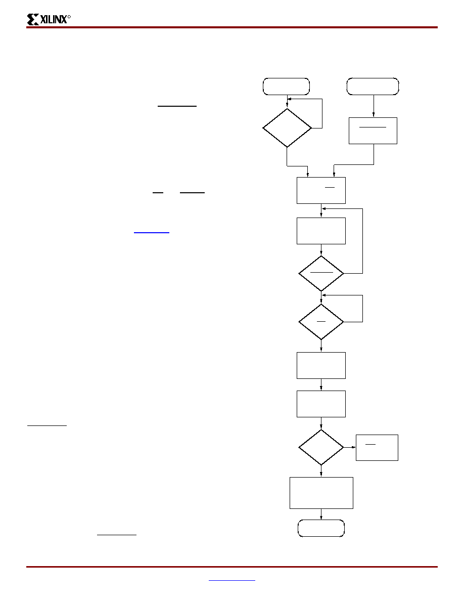
The Process
The sequence of steps necessary to configure Spartan-II
devices are shown in Figure 11. The overall flow can be
divided into three different phases.
Initiating Configuration
Configuration memory clear
Loading data frames
Start-up
The memory clearing and start-up phases are the same for
all configuration modes; however, the steps for the loading
of data frames are different. Thus, the details for data frame
loading are described separately in the sections devoted to
each mode.
Initiating Configuration
There are two different ways to initiate the configuration
process: applying power to the device or asserting the
PROGRAM input.
Configuration on power-up occurs automatically unless it is
delayed by the user, as described in a separate section
below. The waveform for configuration on power-up is
shown in Figure 12, page 19. Before configuration can
begin, VCCO Bank 2 must be greater than 1.0V.
Furthermore, all VCCINT power pins must be connected to a
2.5V supply. For more information on delaying
configuration, see "Clearing Configuration Memory,"
Once in user operation, the device can be re-configured
simply by pulling the PROGRAM pin Low. The device
acknowledges the beginning of the configuration process
by driving DONE Low, then enters the memory-clearing
phase.
Figure 11: Configuration Flow Diagram
FPGA Drives
INIT Low
Abort Start-up
User Holding
INIT
Low?
User Holding
PROGRAM
Low?
FPGA
Drives INIT
and DONE Low
Load
Configuration
Data Frames
User Operation
Configuration
at Power-up
DS001_11_111501
No
CRC
Correct?
Yes
FPGA
Samples
Mode Pins
Delay
Configuration
Delay
Configuration
Clear
Configuration
Memory
User Pulls
PROGRAM
Low
Start-up Sequence
FPGA Drives DONE High,
Activates I/Os,
Releases GSR net
Yes
No
Yes
No
Yes
Configuration During
User Operation
VCCO
AND
VCCINT
High?
相关PDF资料 |
PDF描述 |
|---|---|
| TACR476K002R | CAP TANT 47UF 2V 10% 0805 |
| RMA40DRMI-S288 | CONN EDGECARD 80POS .125 EXTEND |
| XC6SLX9-2TQG144C | IC FPGA SPARTAN-6 9K 144TQFP |
| XC3S200-4TQG144C | IC SPARTAN-3 FPGA 200K 144-TQFP |
| TACR475M020RTA | CAP TANT 4.7UF 20V 20% 0805 |
相关代理商/技术参数 |
参数描述 |
|---|---|
| XC2S50-5FGG256I | 制造商:Xilinx 功能描述:FPGA SPARTAN-II 50K GATES 1728 CELLS 263MHZ 2.5V 256FBGA - Trays |
| XC2S50-5FGG456C | 制造商:XILINX 制造商全称:XILINX 功能描述:Spartan-II FPGA Family |
| XC2S50-5FGG456I | 制造商:XILINX 制造商全称:XILINX 功能描述:Spartan-II FPGA Family |
| XC2S50-5PQ208C | 功能描述:IC FPGA 2.5V 384 CLB'S 208-PQFP RoHS:否 类别:集成电路 (IC) >> 嵌入式 - FPGA(现场可编程门阵列) 系列:Spartan®-II 标准包装:40 系列:Spartan® 6 LX LAB/CLB数:3411 逻辑元件/单元数:43661 RAM 位总计:2138112 输入/输出数:358 门数:- 电源电压:1.14 V ~ 1.26 V 安装类型:表面贴装 工作温度:-40°C ~ 100°C 封装/外壳:676-BGA 供应商设备封装:676-FBGA(27x27) |
| XC2S50-5PQ208I | 功能描述:IC FPGA 2.5V I-TEMP 208-PQFP RoHS:否 类别:集成电路 (IC) >> 嵌入式 - FPGA(现场可编程门阵列) 系列:Spartan®-II 标准包装:40 系列:Spartan® 6 LX LAB/CLB数:3411 逻辑元件/单元数:43661 RAM 位总计:2138112 输入/输出数:358 门数:- 电源电压:1.14 V ~ 1.26 V 安装类型:表面贴装 工作温度:-40°C ~ 100°C 封装/外壳:676-BGA 供应商设备封装:676-FBGA(27x27) |
发布紧急采购,3分钟左右您将得到回复。