参数资料
| 型号: | XC2S50E-6FTG256I |
| 厂商: | Xilinx Inc |
| 文件页数: | 19/108页 |
| 文件大小: | 0K |
| 描述: | IC SPARTAN-IIE FPGA 50K 256FTBGA |
| 产品变化通告: | FPGA Family Discontinuation 18/Apr/2011 |
| 标准包装: | 90 |
| 系列: | Spartan®-IIE |
| LAB/CLB数: | 384 |
| 逻辑元件/单元数: | 1728 |
| RAM 位总计: | 32768 |
| 输入/输出数: | 182 |
| 门数: | 50000 |
| 电源电压: | 1.71 V ~ 1.89 V |
| 安装类型: | 表面贴装 |
| 工作温度: | -40°C ~ 100°C |
| 封装/外壳: | 256-LBGA |
| 供应商设备封装: | 256-FTBGA |
| 其它名称: | 122-1329 |
第1页第2页第3页第4页第5页第6页第7页第8页第9页第10页第11页第12页第13页第14页第15页第16页第17页第18页当前第19页第20页第21页第22页第23页第24页第25页第26页第27页第28页第29页第30页第31页第32页第33页第34页第35页第36页第37页第38页第39页第40页第41页第42页第43页第44页第45页第46页第47页第48页第49页第50页第51页第52页第53页第54页第55页第56页第57页第58页第59页第60页第61页第62页第63页第64页第65页第66页第67页第68页第69页第70页第71页第72页第73页第74页第75页第76页第77页第78页第79页第80页第81页第82页第83页第84页第85页第86页第87页第88页第89页第90页第91页第92页第93页第94页第95页第96页第97页第98页第99页第100页第101页第102页第103页第104页第105页第106页第107页第108页
18
DS077-2 (v3.0) August 9, 2013
Product Specification
Spartan-IIE FPGA Family: Functional Description
R
— OBSOLETE — OBSOLETE — OBSOLETE — OBSOLETE —
edges arrive at internal flip-flops in synchronism with clock
edges arriving at the input.
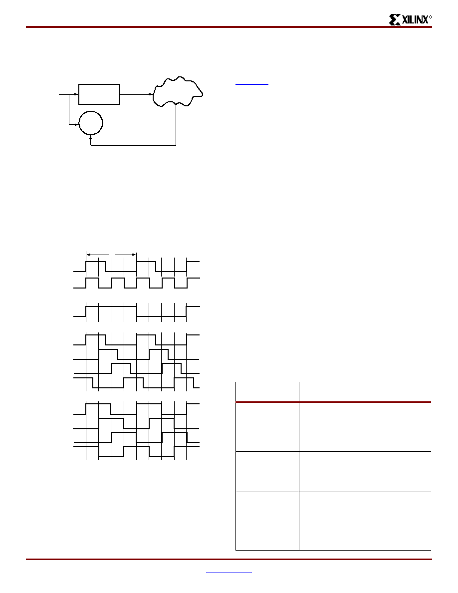
In addition to eliminating clock-distribution delay, the DLL
provides advanced control of multiple clock domains. The
DLL provides four quadrature phases of the source clock,
can double the clock, or divide the clock by 1.5, 2, 2.5, 3, 4,
5, 8, or 16. The phase-shifted output have optional
duty-cycle correction (Figure 13).
The DLL also operates as a clock mirror. By driving the out-
put from a DLL off-chip and then back on again, the DLL can
be used to deskew a board level clock among multiple Spar-
tan-IIE devices.
In order to guarantee that the system clock is operating cor-
rectly prior to the FPGA starting up after configuration, the
DLL can delay the completion of the configuration process
until after it has achieved lock. If the DLL uses external feed-
back, apply a reset after startup to ensure consistent lock-
ing to the external signal. See Xilinx Application Note
XAPP174 for more information on DLLs.
Boundary Scan
Spartan-IIE devices support all the mandatory bound-
ary-scan instructions specified in the IEEE standard 1149.1.
A Test Access Port (TAP) and registers are provided that
implement the EXTEST, INTEST, SAMPLE/PRELOAD,
BYPASS, IDCODE, and HIGHZ instructions. The TAP also
supports two USERCODE instructions, internal scan
chains, and configuration/readback of the device.
The TAP uses dedicated package pins that always operate
using LVTTL. For TDO to operate using LVTTL, the VCCO for
Bank 2 must be 3.3V. Otherwise, TDO switches rail-to-rail
between ground and VCCO. The boundary-scan input pins
(TDI, TMS, TCK) do not have a VCCO requirement and oper-
ate with either 2.5V or 3.3V input signaling levels. TDI, TMS,
and TCK hava a default internal weak pull-up resistor, and
TDO has no default resistor. Bitstream options allow setting
any of the four TAP pins to have an internal pull-up,
pull-down, or neither.
Boundary-scan operation is independent of individual IOB
configurations, and unaffected by package type. All IOBs,
including unbonded ones, are treated as independent
3-state bidirectional pins in a single scan chain. Retention of
the bidirectional test capability after configuration facilitates
the testing of external interconnections.
Table 8 lists the boundary-scan instructions supported in
Spartan-IIE FPGAs. Internal signals can be captured during
EXTEST by connecting them to unbonded or unused IOBs.
They may also be connected to the unused outputs of IOBs
defined as unidirectional input pins.
Figure 12: Delay-Locked Loop Block Diagram
Figure 13: DLL Output Characteristics
Clock
Distribution
Network
Variable
Delay Line
CLKOUT
Control
CLKFB
CLKIN
ds077-2_10_070203
x132_07_092599
CLKIN
CLK2X
CLK0
CLK90
CLK180
CLK270
CLKDV
CLKDV_DIVIDE=2
DUTY_CYCLE_CORRECTION=FALSE
CLK0
CLK90
CLK180
CLK270
DUTY_CYCLE_CORRECTION=TRUE
t
0
90 180 270
0
90 180 270
Table 8: Boundary-Scan Instructions
Boundary-Scan
Command
Binary
Code[4:0]
Description
EXTEST
00000
Enables boundary-scan
EXTEST operation
SAMPLE/
PRELOAD
00001
Enables boundary-scan
SAMPLE/PRELOAD
operation
USER1
00010
Access user-defined
register 1
USER2
00011
Access user-defined
register 2
CFG_OUT
00100
Access the
configuration bus for
Readback
CFG_IN
00101
Access the
configuration bus for
Configuration
相关PDF资料 |
PDF描述 |
|---|---|
| EHHD15MFB | CONN DSUB 15PIN MALE-FMALE BLK |
| 24LCS52T-I/MC | IC EEPROM 2KBIT 400KHZ 8DFN |
| XC2S100-6PQ208C | IC FPGA 2.5V C-TEMP 208-PQFP |
| ACC60DREI | CONN EDGECARD 120PS .100 EYELET |
| XC2S100-5PQ208I | IC FPGA 2.5V I-TEMP 208-PQFP |
相关代理商/技术参数 |
参数描述 |
|---|---|
| XC2S50E-6PQ208C | 功能描述:IC FPGA 1.8V 384 CLB'S 208-PQFP RoHS:否 类别:集成电路 (IC) >> 嵌入式 - FPGA(现场可编程门阵列) 系列:Spartan®-IIE 标准包装:40 系列:Spartan® 6 LX LAB/CLB数:3411 逻辑元件/单元数:43661 RAM 位总计:2138112 输入/输出数:358 门数:- 电源电压:1.14 V ~ 1.26 V 安装类型:表面贴装 工作温度:-40°C ~ 100°C 封装/外壳:676-BGA 供应商设备封装:676-FBGA(27x27) |
| XC2S50E-6PQ208I | 制造商:Xilinx 功能描述:IC SPARTAN-IIE FPGA 50K 208-PQFP 制造商:Xilinx 功能描述:IC FPGA 146 I/O 208PQFP |
| XC2S50E-6PQG208C | 功能描述:IC SPARTAN-IIE FPGA 50K 208-PQFP RoHS:是 类别:集成电路 (IC) >> 嵌入式 - FPGA(现场可编程门阵列) 系列:Spartan®-IIE 标准包装:24 系列:ECP2 LAB/CLB数:1500 逻辑元件/单元数:12000 RAM 位总计:226304 输入/输出数:131 门数:- 电源电压:1.14 V ~ 1.26 V 安装类型:表面贴装 工作温度:0°C ~ 85°C 封装/外壳:208-BFQFP 供应商设备封装:208-PQFP(28x28) |
| XC2S50E-6PQG208I | 制造商:XILINX 制造商全称:XILINX 功能描述:Spartan-IIE FPGA |
| XC2S50E-6TQ144C | 功能描述:IC FPGA 1.8V 384 CLB'S 144-TQFP RoHS:否 类别:集成电路 (IC) >> 嵌入式 - FPGA(现场可编程门阵列) 系列:Spartan®-IIE 标准包装:40 系列:Spartan® 6 LX LAB/CLB数:3411 逻辑元件/单元数:43661 RAM 位总计:2138112 输入/输出数:358 门数:- 电源电压:1.14 V ~ 1.26 V 安装类型:表面贴装 工作温度:-40°C ~ 100°C 封装/外壳:676-BGA 供应商设备封装:676-FBGA(27x27) |
发布紧急采购,3分钟左右您将得到回复。