参数资料
| 型号: | XC3020A-7PC84C |
| 厂商: | Xilinx Inc |
| 文件页数: | 45/76页 |
| 文件大小: | 0K |
| 描述: | IC LOGIC CL ARRAY 2000GAT 84PLCC |
| 产品变化通告: | Product Discontinuation 27/Apr/2010 |
| 标准包装: | 1 |
| 系列: | XC3000A/L |
| LAB/CLB数: | 64 |
| RAM 位总计: | 14779 |
| 输入/输出数: | 64 |
| 门数: | 1500 |
| 电源电压: | 4.75 V ~ 5.25 V |
| 安装类型: | 表面贴装 |
| 工作温度: | 0°C ~ 85°C |
| 封装/外壳: | 84-LCC(J 形引线) |
| 供应商设备封装: | 84-PLCC |
| 其它名称: | 122-1010 |
第1页第2页第3页第4页第5页第6页第7页第8页第9页第10页第11页第12页第13页第14页第15页第16页第17页第18页第19页第20页第21页第22页第23页第24页第25页第26页第27页第28页第29页第30页第31页第32页第33页第34页第35页第36页第37页第38页第39页第40页第41页第42页第43页第44页当前第45页第46页第47页第48页第49页第50页第51页第52页第53页第54页第55页第56页第57页第58页第59页第60页第61页第62页第63页第64页第65页第66页第67页第68页第69页第70页第71页第72页第73页第74页第75页第76页
R
November 9, 1998 (Version 3.1)
7-7
XC3000 Series Field Programmable Gate Arrays
7
The memory cell outputs Q and Q use ground and VCC lev-
els and provide continuous, direct control. The additional
capacitive load together with the absence of address
decoding and sense amplifiers provide high stability to the
cell. Due to the structure of the configuration memory cells,
they are not affected by extreme power-supply excursions
or very high levels of alpha particle radiation. In reliability
testing, no soft errors have been observed even in the
presence of very high doses of alpha radiation.
The method of loading the configuration data is selectable.
Two methods use serial data, while three use byte-wide
data. The internal configuration logic utilizes framing infor-
mation, embedded in the program data by the development
system, to direct memory-cell loading. The serial-data
framing and length-count preamble provide programming
compatibility for mixes of various FPGA device devices in a
synchronous, serial, daisy-chain fashion.
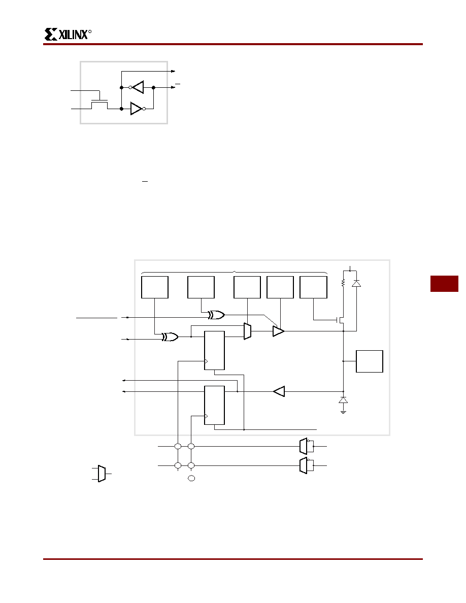
I/O Block
Each user-configurable IOB shown in Figure 4, provides an
interface between the external package pin of the device
and the internal user logic. Each IOB includes both regis-
tered and direct input paths. Each IOB provides a program-
mable 3-state output buffer, which may be driven by a
registered or direct output signal. Configuration options
allow each IOB an inversion, a controlled slew rate and a
high impedance pull-up. Each input circuit also provides
input clamping diodes to provide electrostatic protection,
and circuits to inhibit latch-up produced by input currents.
Q
Data
Read or
Write
Configuration
Control
Q
X5382
Figure 3: Static Configuration Memory Cell.
It is loaded with one bit of configuration program and con-
trols one program selection in the Field Programmable
Gate Array.
FLIP
FLOP
Q
D
R
SLEW
RATE
PASSIVE
PULL UP
OUTPUT
SELECT
3-STATE
INVERT
OUT
INVERT
FLIP
FLOP
or
LATCH
D
Q
R
REGISTERED IN
DIRECT IN
OUT
3- STATE
(OUTPUT ENABLE)
TTL or
CMOS
INPUT
THRESHOLD
OUTPUT
BUFFER
(GLOBAL RESET)
CK1
X3029
I/O PAD
Vcc
PROGRAM-CONTROLLED MEMORY CELLS
PROGRAMMABLE INTERCONNECTION POINT or PIP
=
IK
OK
Q
I
O
T
PROGRAM
CONTROLLED
MULTIPLEXER
CK2
Figure 4: Input/Output Block.
Each IOB includes input and output storage elements and I/O options selected by configuration memory cells. A choice
of two clocks is available on each die edge. The polarity of each clock line (not each flip-flop or latch) is programmable.
A clock line that triggers the flip-flop on the rising edge is an active Low Latch Enable (Latch transparent) signal and vice
versa. Passive pull-up can only be enabled on inputs, not on outputs. All user inputs are programmed for TTL or CMOS
thresholds.
Product Obsolete or Under Obsolescence
相关PDF资料 |
PDF描述 |
|---|---|
| ASM43DTMS-S189 | CONN EDGECARD 86POS R/A .156 SLD |
| XC3030A-7PC84C | IC LOGIC CL ARRAY 3000GAT 84PLCC |
| AGM43DTMS-S189 | CONN EDGECARD 86POS R/A .156 SLD |
| AYM43DTBS-S189 | CONN EDGECARD 86POS R/A .156 SLD |
| ASM43DTBS-S189 | CONN EDGECARD 86POS R/A .156 SLD |
相关代理商/技术参数 |
参数描述 |
|---|---|
| XC3020A-7PC84C0100 | 制造商:Xilinx 功能描述: |
| XC3020A-7PC84I | 制造商:Xilinx 功能描述: |
| XC3020A-7PCG68C | 制造商:Xilinx 功能描述: |
| XC3020A-7PQ100C | 制造商:XILINX 制造商全称:XILINX 功能描述:Field Programmable Gate Arrays (XC3000A/L, XC3100A/L) |
| XC3020A-7PQ100I | 制造商:Xilinx 功能描述: |
发布紧急采购,3分钟左右您将得到回复。