参数资料
| 型号: | XC3020A-7PC84C |
| 厂商: | Xilinx Inc |
| 文件页数: | 49/76页 |
| 文件大小: | 0K |
| 描述: | IC LOGIC CL ARRAY 2000GAT 84PLCC |
| 产品变化通告: | Product Discontinuation 27/Apr/2010 |
| 标准包装: | 1 |
| 系列: | XC3000A/L |
| LAB/CLB数: | 64 |
| RAM 位总计: | 14779 |
| 输入/输出数: | 64 |
| 门数: | 1500 |
| 电源电压: | 4.75 V ~ 5.25 V |
| 安装类型: | 表面贴装 |
| 工作温度: | 0°C ~ 85°C |
| 封装/外壳: | 84-LCC(J 形引线) |
| 供应商设备封装: | 84-PLCC |
| 其它名称: | 122-1010 |
第1页第2页第3页第4页第5页第6页第7页第8页第9页第10页第11页第12页第13页第14页第15页第16页第17页第18页第19页第20页第21页第22页第23页第24页第25页第26页第27页第28页第29页第30页第31页第32页第33页第34页第35页第36页第37页第38页第39页第40页第41页第42页第43页第44页第45页第46页第47页第48页当前第49页第50页第51页第52页第53页第54页第55页第56页第57页第58页第59页第60页第61页第62页第63页第64页第65页第66页第67页第68页第69页第70页第71页第72页第73页第74页第75页第76页
R
November 9, 1998 (Version 3.1)
7-55
XC3000 Series Field Programmable Gate Arrays
7
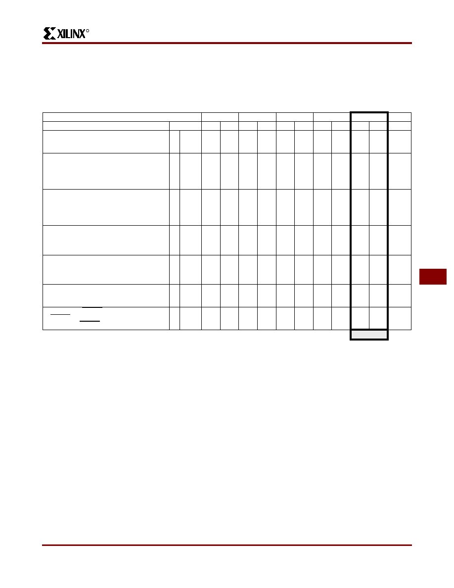
XC3100A CLB Switching Characteristics Guidelines
Testing of the switching parameters is modeled after testing methods specified by MIL-M-38510/605. All devices are 100%
functionally tested. Since many internal timing parameters cannot be measured directly, they are derived from benchmark
timing patterns. The following guidelines reflect worst-case values over the recommended operating conditions. For more
detailed, more precise, and more up-to-date timing information, use the values provided by the timing calculator and used
in the simulator.
Notes: 1. The CLB K to Q output delay (TCKO, #8) of any CLB, plus the shortest possible interconnect delay, is always longer than the
Data In hold time requirement (TCKDI, #5) of any CLB on the same die.
2. TILO, TQLO and TICK are specified for 4-input functions. For 5-input functions or base FGM functions, each of these
specifications for the XC3100A family increases by 0.50 ns (-5), 0.42 ns (-4) and 0.35 ns (-3), 0.35 ns (-2), 0.30 ns (-1), and
0.30 ns (-09).
Speed Grade
-4-3-2-1
-09
Description
Symbol
Min
Max
Min
Max
Min
Max
Min
Max
Min
Max
Units
Combinatorial Delay
Logic Variables
A, B, C, D, E,
to outputs X or Y
1TILO
3.3
2.7
2.2
1.75
1.5
ns
Sequential delay
Clock k to outputs X or Y
Clock k to outputs X or Y when Q is returned
through function generators F or G to drive
X or Y
8TCKO
TQLO
2.5
5.2
2.1
4.3
1.7
3.5
1.4
3.1
1.25
2.7
ns
Set-up time before clock K
Logic Variables
A, B, C, D, E
Data In
DI
Enable Clock
EC
Reset Direct inactive
RD
2
4
6
TICK
TDICK
TECCK
2.5
1.6
3.2
1.0
2.1
1.4
2.7
1.0
1.8
1.3
2.5
1.0
1.7
1.2
2.3
1.0
1.5
1.0
2.05
1.0
ns
Hold Time after clock K
Logic Variables
A, B, C, D, E
Data In
DI
Enable Clock
EC
3
5
7
TCKI
TCKDI
TCKEC
0
1.0
0.8
0
0.9
0.7
0
0.9
0.7
0
0.8
0.6
0
0.7
0.55
ns
Clock
Clock High time
Clock Low time
Max. flip-flop toggle rate
11
12
TCH
TCL
FCLK
2.0
227
1.6
270
1.3
323
1.3
323
1.3
370
ns
MHz
Reset Direct (RD)
RD width
delay from RD to outputs X or Y
13
9
TRPW
TRIO
3.2
3.7
2.7
3.1
2.3
2.7
2.3
2.4
2.05
2.15
ns
Global Reset (RESET Pad)1
RESET width (Low)
(XC3142A)
delay from RESET pad to outputs X or Y
TMRW
TMRQ
14.0
12.0
ns
Prelim
Product Obsolete or Under Obsolescence
相关PDF资料 |
PDF描述 |
|---|---|
| ASM43DTMS-S189 | CONN EDGECARD 86POS R/A .156 SLD |
| XC3030A-7PC84C | IC LOGIC CL ARRAY 3000GAT 84PLCC |
| AGM43DTMS-S189 | CONN EDGECARD 86POS R/A .156 SLD |
| AYM43DTBS-S189 | CONN EDGECARD 86POS R/A .156 SLD |
| ASM43DTBS-S189 | CONN EDGECARD 86POS R/A .156 SLD |
相关代理商/技术参数 |
参数描述 |
|---|---|
| XC3020A-7PC84C0100 | 制造商:Xilinx 功能描述: |
| XC3020A-7PC84I | 制造商:Xilinx 功能描述: |
| XC3020A-7PCG68C | 制造商:Xilinx 功能描述: |
| XC3020A-7PQ100C | 制造商:XILINX 制造商全称:XILINX 功能描述:Field Programmable Gate Arrays (XC3000A/L, XC3100A/L) |
| XC3020A-7PQ100I | 制造商:Xilinx 功能描述: |
发布紧急采购,3分钟左右您将得到回复。