参数资料
| 型号: | XC3020A-7PC84C |
| 厂商: | Xilinx Inc |
| 文件页数: | 7/76页 |
| 文件大小: | 0K |
| 描述: | IC LOGIC CL ARRAY 2000GAT 84PLCC |
| 产品变化通告: | Product Discontinuation 27/Apr/2010 |
| 标准包装: | 1 |
| 系列: | XC3000A/L |
| LAB/CLB数: | 64 |
| RAM 位总计: | 14779 |
| 输入/输出数: | 64 |
| 门数: | 1500 |
| 电源电压: | 4.75 V ~ 5.25 V |
| 安装类型: | 表面贴装 |
| 工作温度: | 0°C ~ 85°C |
| 封装/外壳: | 84-LCC(J 形引线) |
| 供应商设备封装: | 84-PLCC |
| 其它名称: | 122-1010 |
第1页第2页第3页第4页第5页第6页当前第7页第8页第9页第10页第11页第12页第13页第14页第15页第16页第17页第18页第19页第20页第21页第22页第23页第24页第25页第26页第27页第28页第29页第30页第31页第32页第33页第34页第35页第36页第37页第38页第39页第40页第41页第42页第43页第44页第45页第46页第47页第48页第49页第50页第51页第52页第53页第54页第55页第56页第57页第58页第59页第60页第61页第62页第63页第64页第65页第66页第67页第68页第69页第70页第71页第72页第73页第74页第75页第76页
R
November 9, 1998 (Version 3.1)
7-17
XC3000 Series Field Programmable Gate Arrays
7
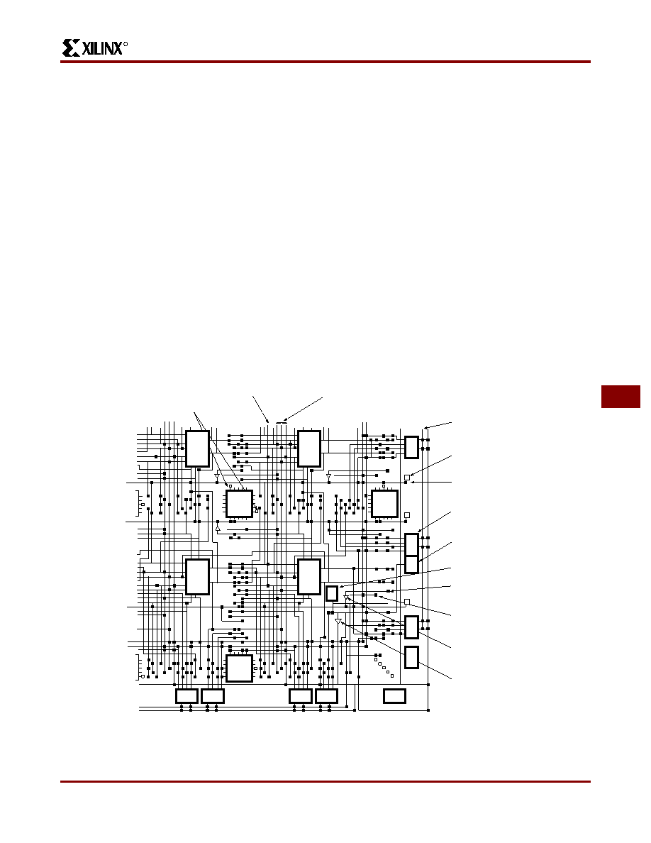
A buffer in the upper left corner of the FPGA chip drives a
global net which is available to all K inputs of logic blocks.
Using the global buffer for a clock signal provides a
skew-free, high fan-out, synchronized clock for use at any
or all of the IOBs and CLBs. Configuration bits for the K
input to each logic block can select this global line or
another routing resource as the clock source for its
flip-flops. This net may also be programmed to drive the die
edge clock lines for IOB use. An enhanced speed, CMOS
threshold, direct access to this buffer is available at the sec-
ond pad from the top of the left die edge.
A buffer in the lower right corner of the array drives a hori-
zontal Longline that can drive programmed connections to
a vertical Longline in each interconnection column. This
alternate buffer also has low skew and high fan-out. The
network formed by this alternate buffer’s Longlines can be
selected to drive the K inputs of the CLBs. CMOS thresh-
old, high speed access to this buffer is available from the
third pad from the bottom of the right die edge.
Internal Busses
A pair of 3-state buffers, located adjacent to each CLB, per-
mits logic to drive the horizontal Longlines. Logic operation
of the 3-state buffer controls allows them to implement wide
multiplexing functions. Any 3-state buffer input can be
selected as drive for the horizontal long-line bus by apply-
ing a Low logic level on its 3-state control line. See
Figure 16. The user is required to avoid contention which
can result from multiple drivers with opposing logic levels.
Control of the 3-state input by the same signal that drives
the buffer input, creates an open-drain wired-AND function.
A logic High on both buffer inputs creates a high imped-
ance, which represents no contention. A logic Low enables
the buffer to drive the Longline Low. See Figure 17. Pull-up
resistors are available at each end of the Longline to pro-
vide a High output when all connected buffers are non-con-
ducting. This forms fast, wide gating functions. When data
drives the inputs, and separate signals drive the 3-state
control lines, these buffers form multiplexers (3-state bus-
ses). In this case, care must be used to prevent contention
through multiple active buffers of conflicting levels on a
common line. Each horizontal Longline is also driven by a
weak keeper circuit that prevents undefined floating levels
by maintaining the previous logic level when the line is not
driven by an active buffer or a pull-up resistor. Figure 18
shows 3-state buffers, Longlines and pull-up resistors.
3-STATE CONTROL
GG
HG
P40
P41
P42
P43
RST
P46
.l
X1245
.q
.Q
OS
C
P47
BCL
KIN
P48
GH
HH
.lk
.ck
I/O CLOCKS
BIDIRECTIONAL
INTERCONNECT
BUFFERS
GLOBAL NET
3 VERTICAL LONG
LINES PER COLUMN
HORIZONTAL LONG LINE
PULL-UP RESISTOR
HORIZONTAL LONG LINE
OSCILLATOR
AMPLIFIER OUTPUT
DIRECTINPUT OF P47
TO AUXILIARY BUFFER
CRYSTAL OSCILLATOR
BUFFER
3-STATE INPUT
3-STATE BUFFER
ALTERNATE BUFFER
D
P
G
M
Figure 18: Design Editor.
An extra large view of possible interconnections in the lower right corner of the XC3020A.
Product Obsolete or Under Obsolescence
相关PDF资料 |
PDF描述 |
|---|---|
| ASM43DTMS-S189 | CONN EDGECARD 86POS R/A .156 SLD |
| XC3030A-7PC84C | IC LOGIC CL ARRAY 3000GAT 84PLCC |
| AGM43DTMS-S189 | CONN EDGECARD 86POS R/A .156 SLD |
| AYM43DTBS-S189 | CONN EDGECARD 86POS R/A .156 SLD |
| ASM43DTBS-S189 | CONN EDGECARD 86POS R/A .156 SLD |
相关代理商/技术参数 |
参数描述 |
|---|---|
| XC3020A-7PC84C0100 | 制造商:Xilinx 功能描述: |
| XC3020A-7PC84I | 制造商:Xilinx 功能描述: |
| XC3020A-7PCG68C | 制造商:Xilinx 功能描述: |
| XC3020A-7PQ100C | 制造商:XILINX 制造商全称:XILINX 功能描述:Field Programmable Gate Arrays (XC3000A/L, XC3100A/L) |
| XC3020A-7PQ100I | 制造商:Xilinx 功能描述: |
发布紧急采购,3分钟左右您将得到回复。