参数资料
| 型号: | XC3042A-7PQ100C |
| 厂商: | Xilinx Inc |
| 文件页数: | 76/76页 |
| 文件大小: | 0K |
| 描述: | IC LOGIC CL ARRAY 4200GAT 100PQF |
| 产品变化通告: | Product Discontinuation 27/Apr/2010 |
| 标准包装: | 1 |
| 系列: | XC3000A/L |
| LAB/CLB数: | 144 |
| RAM 位总计: | 30784 |
| 输入/输出数: | 82 |
| 门数: | 3000 |
| 电源电压: | 4.75 V ~ 5.25 V |
| 安装类型: | 表面贴装 |
| 工作温度: | 0°C ~ 85°C |
| 封装/外壳: | 100-BQFP |
| 供应商设备封装: | 100-QFP(14x20) |
| 其它名称: | 122-1026 |
第1页第2页第3页第4页第5页第6页第7页第8页第9页第10页第11页第12页第13页第14页第15页第16页第17页第18页第19页第20页第21页第22页第23页第24页第25页第26页第27页第28页第29页第30页第31页第32页第33页第34页第35页第36页第37页第38页第39页第40页第41页第42页第43页第44页第45页第46页第47页第48页第49页第50页第51页第52页第53页第54页第55页第56页第57页第58页第59页第60页第61页第62页第63页第64页第65页第66页第67页第68页第69页第70页第71页第72页第73页第74页第75页当前第76页
R
November 9, 1998 (Version 3.1)
7-11
XC3000 Series Field Programmable Gate Arrays
7
General Purpose Interconnect
General purpose interconnect, as shown in Figure 10, con-
sists of a grid of five horizontal and five vertical metal seg-
ments located between the rows and columns of logic and
IOBs. Each segment is the height or width of a logic block.
Switching matrices join the ends of these segments and
allow programmed interconnections between the metal grid
segments of adjoining rows and columns. The switches of
an unprogrammed device are all non-conducting. The con-
nections through the switch matrix may be established by
the automatic routing or by selecting the desired pairs of
matrix pins to be connected or disconnected. The legiti-
mate switching matrix combinations for each pin are indi-
cated in Figure 11.
Special buffers within the general interconnect areas pro-
vide periodic signal isolation and restoration for improved
performance of lengthy nets. The interconnect buffers are
available to propagate signals in either direction on a given
general interconnect segment. These bidirectional (bidi)
buffers are found adjacent to the switching matrices, above
and to the right. The other PIPs adjacent to the matrices
are accessed to or from Longlines. The development sys-
tem automatically defines the buffer direction based on the
location of the interconnection network source. The delay
calculator of the development system automatically calcu-
lates and displays the block, interconnect and buffer delays
for any paths selected. Generation of the simulation netlist
with a worst-case delay model is provided.
Direct Interconnect
Direct interconnect, shown in Figure 12, provides the most
efficient implementation of networks between adjacent
CLBs or I/O Blocks. Signals routed from block to block
using the direct interconnect exhibit minimum interconnect
propagation and use no general interconnect resources.
For each CLB, the X output may be connected directly to
the B input of the CLB immediately to its right and to the C
input of the CLB to its left. The Y output can use direct inter-
connect to drive the D input of the block immediately above
and the A input of the block below. Direct interconnect
should be used to maximize the speed of high-performance
portions of logic. Where logic blocks are adjacent to IOBs,
direct connect is provided alternately to the IOB inputs (I)
and outputs (O) on all four edges of the die. The right edge
provides additional direct connects from CLB outputs to
adjacent IOBs. Direct interconnections of IOBs with CLBs
are shown in Figure 13.
D
Q
D
Q
D
Q
Count Enable
Parallel Enable
Clock
D2
D1
D0
Dual Function of 4 Variables
Function of 6 Variables
Function of 5 Variables
Q2
Q1
Q0
FG
Mode
F
Mode
FGM
Mode
Terminal
Count
X5383
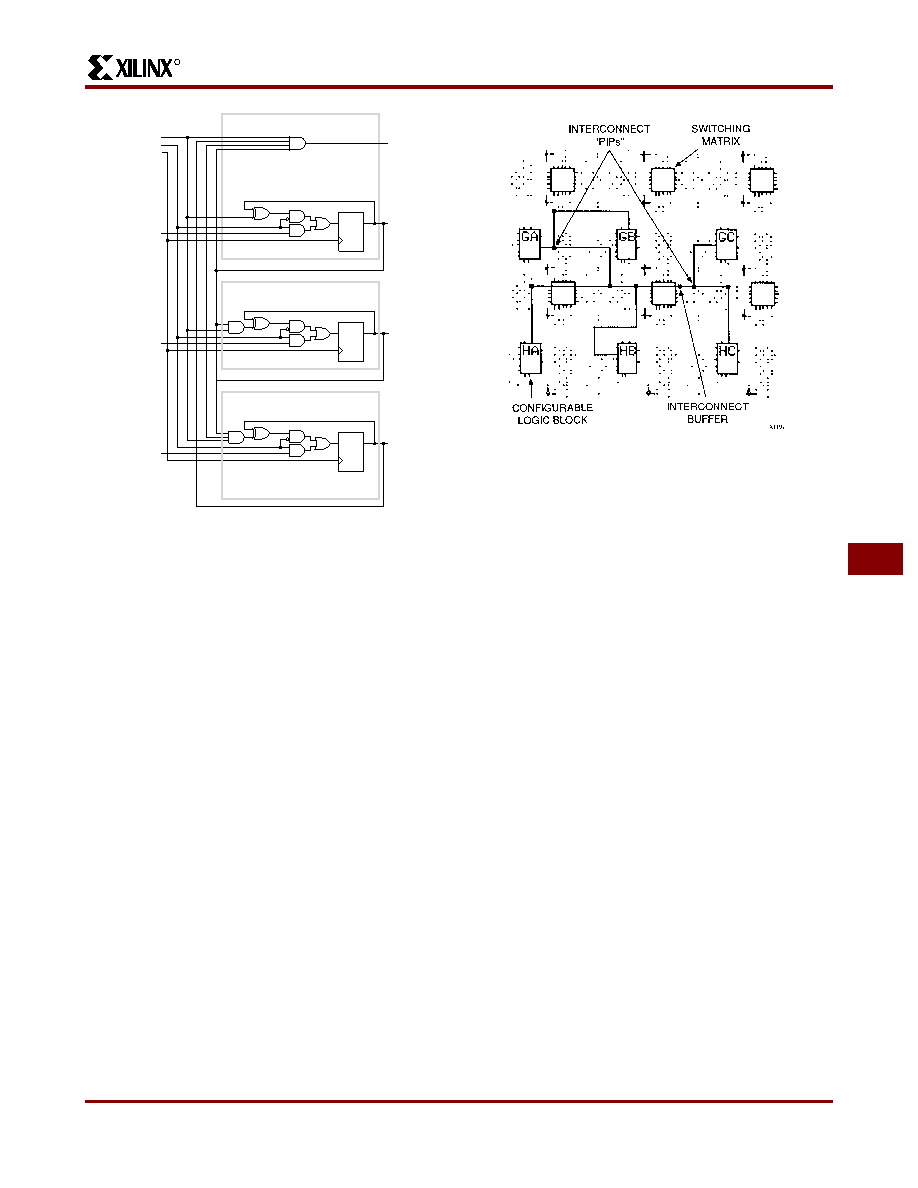
Figure 7: Counter.
The modulo-8 binary counter with parallel enable and
clock enable uses one combinatorial logic block of each
option.
Figure 8: A Design Editor view of routing resources
used to form a typical interconnection network from
CLB GA.
Product Obsolete or Under Obsolescence
相关PDF资料 |
PDF描述 |
|---|---|
| ABC65DRES-S734 | CONN EDGECARD 130PS .100 EYELET |
| A14V40A-PQG160C | IC FPGA 4K GATES 3.3V 160-PQFP |
| EMC18DTEF | CONN EDGECARD 36POS .100 EYELET |
| A1425A-1PQ160I | IC FPGA 2500 GATES 160-PQFP |
| A1440A-PQG160I | IC FPGA 4K GATES 160-PQFP |
相关代理商/技术参数 |
参数描述 |
|---|---|
| XC3042A-7PQ100C0167 | 制造商:Xilinx 功能描述: |
| XC3042A-7PQ100C0262 | 制造商:Xilinx 功能描述: |
| XC3042A-7PQ100C0341 | 制造商:Xilinx 功能描述: |
| XC3042A-7PQ100I | 制造商: 功能描述: 制造商:undefined 功能描述: |
| XC3042A-7PQG100I | 制造商:Xilinx 功能描述: |
发布紧急采购,3分钟左右您将得到回复。